TOPCon vs. HJT Solar Cells | Which is More Efficient
HJT mass production efficiency leads the way exceeding 26%, and its 90% bifaciality factor and -0.26%/C temperature coefficient increase power generation in high temperatures by 8%.
Procurement recommendation: HJT is the first choice for extreme high temperatures or space-constrained areas;
For general-purpose projects, choose TOPCon to achieve the optimal system LCOE by taking advantage of its 25.5% efficiency and mature supply chain.
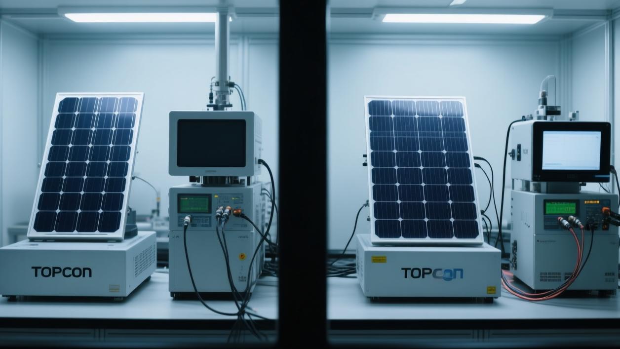
Mass Production Efficiency
Current mass production data shows that the average efficiency of TOPCon cells is distributed between 25.5% - 26.2%, relying on a 1.5 nm oxide layer and a polysilicon layer to reduce recombination losses.
The average efficiency of HJT cells on the production line reaches 25.8% - 26.6%, with their open-circuit voltages generally exceeding 745 mV.
HJT features a bifaciality factor of over 90% and a temperature coefficient of -0.26%/°C, resulting in higher actual power generation in high-temperature environments compared to TOPCon (which has a bifaciality of about 80%-85% and a temperature coefficient of -0.30%/°C).
TOPCon
The TOPCon structure achieves passivation by preparing an ultra-thin silicon dioxide layer of 1.2 nm to 1.5 nm on the rear side of the silicon wafer. The subsequently deposited doped polysilicon layer is usually controlled at a thickness of 20 nm to 50 nm. This configuration reduces the surface recombination velocity to below 10 fA/cm², laying the physical foundation for mass production efficiency to break through 26%.
In terms of light sensing and capture, the front side retains the traditional pyramid texturing, increasing the short-circuit current by controlling the reflectivity to 1% to 2.5%. Although the rear polysilicon layer provides excellent electrical properties, there is parasitic absorption loss in the 300 nm to 600 nm band. To optimize the metrics, mass production lines have begun attempting to thin the polysilicon layer down to 20 nm, increasing efficiency by about 0.1%.
The Voc (open-circuit voltage) performance in mass production is stable in the 715 mV to 730 mV range. Compared to the 680 mV of PERC technology, this leap stems from the selective collection of carriers by the tunneling oxide layer. By precisely controlling the doping concentration of phosphorus atoms in the polysilicon to reach 10^20 cm⁻³, conductivity can be optimized without increasing absorption losses.
The current mainstream deposition processes are divided into three routes. LPCVD occupies about 70% of the existing global production capacity due to its high film quality and thickness uniformity controlled within ±3%. PECVD is favored for its single-machine throughput of 8000 wafers/hour and lower wrap-around deposition ratio, while PEALD technology reaches a thickness precision level of 0.1 nm.
l Passivation Quality: Minority carrier lifetime in the mass production stage is generally required to reach over 3.5 ms to ensure charge collection efficiency.
l Sheet Resistance Parameters: The sheet resistance after the diffusion process stabilizes at 140 ± 10 Ω/sq, reducing lateral transmission resistance.
l Paste Consumption: Through fine-line screen printing technology, the silver paste consumption per unit drops to 10.5 mg/W, lowering non-silicon expenditures.
l LECO Efficiency Gain: Laser Enhanced Contact Optimization (LECO) technology reduces contact resistance by about 80%, achieving a conversion efficiency gain of 0.25%.
l Grid Line Dimensions: The width of the fine grid lines after paste printing is maintained at 24 μm, reducing the shading area ratio to below 3%.
The Fill Factor (FF) is another indicator for measuring mass production levels, and the production line can now stably achieve levels of 83% to 84.5%. This benefits from the optimization of the ohmic contact formed between the metallization paste and the polysilicon layer. By using silver-aluminum paste containing specific glass frit modules, metal contact points about 10 nm deep can be formed at a sintering temperature around 750°C.
In terms of temperature rise characteristics, the temperature coefficient of TOPCon is about -0.30%/°C. When the ambient temperature rises to 45°C, its output power degradation is reduced by about 0.6% compared to traditional PERC. The bifaciality factor remains at 80% to 85%, which means that on highly reflective underlying surfaces like grass, the rear-side gain can contribute about 12% of the total power generation.
Performance at the module end also reflects the efficiency advantage. The power of a 182mm 72-cell format module has reached 585W to 595W. By adopting SMBB (Super Multi-Busbar) technology and using 16 or more circular ribbons, the current transmission distance on the fine grid lines is shortened, keeping the module encapsulation loss controlled at around 1.0%.
l Yield Control: The current yield rate of TOPCon production lines for mainstream global enterprises has stabilized between 97.5% and 98.2%.
l Degradation Level: First-year Light-Induced Degradation (LID) is below 1.0%, and annual degradation is controlled at the 0.4% level.
l Module Weight: Adopting a 1.6mm + 1.6mm half-cut double-glass design keeps the weight per unit area below 12 kg/m².
l Low Irradiance Gain: Due to the passivation layer's ability to retain weak currents, its efficiency retention rate exceeds 95% under 200 W/m² low light.
l Wafer Thickness: The mass production end is transitioning from 150μm to 130μm, reducing silicon consumption per watt by about 0.15 g.
In the actual production rhythm, a 1GW scale production line can produce over 220,000 cells per day. The production time for a single cell is about 1.6 seconds, and this high-throughput manufacturing capability keeps it competitive. The current process flow is simplified to 12 to 14 steps, mainly concentrated on the alternating growth of boron diffusion and the tunneling oxide layer.
Addressing front-side reflection losses, the mass production process introduces a double-layer anti-reflective coating (ARC), composed of a silicon nitride and aluminum oxide composite. The aluminum oxide layer not only provides chemical passivation but also repels minority carriers through a field-effect passivation mechanism. This composite film layer suppresses the reflectivity in the blue light band to within 5%, increasing the total capture of sunlight.
Double Sided Poly is the evolutionary direction for the next stage. By introducing the same passivation structure on the front side, mass production efficiency is expected to be pushed to 26.8%. Initial tests show that this technology can further increase Voc to 740 mV. The current challenge lies in the optical loss of the front-side polysilicon layer, which requires precise thickness control within 10 nm.
l Contact Resistance: The resistivity at the metal and semiconductor interface is controlled at the 1 mΩ·cm² magnitude, reducing heat loss.
l Doping Depth: The distribution depth of phosphorus atoms in the polysilicon is about 150 nm, ensuring the continuity of conductivity.
l Oxygen Content Index: The internal oxygen content of the silicon wafer must be below 10 ppma, reducing precipitation risks during high-temperature processes.
l Carbon Content Control: The carbon content of the silicon wafer must be below 0.5 ppm to prevent affecting lattice integrity.
l Micro-crack Rate: Through Automated Optical Inspection (AOI), the detection rate of micro-cracks in mass production is required to be below 0.1%.
The choice of materials at the encapsulation end also affects efficiency performance. To match the sensitivity of N-type cells to moisture, mass-produced modules widely adopt POE (Polyolefin Elastomer) film. The Water Vapor Transmission Rate (WVTR) of this material is below 0.5 g/m²·day, preventing acetic acid from corroding the metal grids. Over a 30-year lifecycle, this configuration ensures power output.
Current equipment investment (CAPEX) has dropped to around 140 million RMB/GW. A single tubular oxidation equipment can process over 400 wafers simultaneously, achieving large-scale output through a multi-tube parallel mode. This maturity enables TOPCon to complete a global capacity deployment of over 500 GW within a short period.
HJT
The HJT structure uses an N-type monocrystalline silicon wafer as the substrate, depositing 5 nm to 10 nm thick intrinsic amorphous silicon (i-a-Si: H) films on both sides of the wafer. This thin film acts as an excellent passivation layer, suppressing the surface recombination current density to below 5 fA/cm². The resulting physical barrier gives charge carriers a longer survival time before collection; typically, minority carrier lifetime in mass production needs to exceed 5 ms.
Following the intrinsic layer are doped amorphous silicon layers, forming p-type and n-type contacts respectively. This p-i-n structure is the source of high open-circuit voltage (Voc). In standard production workflows, Voc readings generally fall between 745 mV and 755 mV, significantly outperforming traditional high-temperature diffusion technologies. Because the temperature throughout the entire deposition process remains below 200°C, the internal lattice structure of the silicon wafer is not thermally damaged, preserving the material's intrinsic quality.
Due to the weak conductivity of the amorphous silicon layer, an 80 nm thick transparent conductive oxide (TCO) layer must be coated on both sides via a sputtering process, usually using Indium Tin Oxide (ITO). The sheet resistance of this film must be precisely controlled at around 100 Ω/sq to balance optical transmittance and lateral conductivity. This design ensures that the Fill Factor (FF) can stabilize at high levels of 84% to 85.5%.
Currently, production lines are transitioning toward a microcrystalline process by replacing traditional amorphous silicon with microcrystalline silicon (μc-Si: H). The microcrystalline silicon layer has a wider optical bandgap, reducing light absorption loss at short wavelengths and increasing the short-circuit current (Jsc) by about 0.6 mA/cm². This technological evolution directly leaps the average mass production conversion efficiency of HJT from 25.8% to over 26.5%.
l Process Steps: The entire line requires only 4 to 6 steps, shortening the production cycle to under 30 minutes.
l Deposition Speed: PECVD equipment can process over 6000 wafers per hour, with thickness uniformity controlled at ±2%.
l Target Utilization: The indium target utilization rate in the PVD process has been increased to 80% through rotary target technology.
l Wafer Thickness: Laboratories have verified the mass production feasibility of 110 μm thickness, reducing silicon consumption per watt by about 20%.
l Low-Temperature Advantage: Due to the absence of a high-temperature annealing step, the warpage of the silicon wafer during processing is below 0.5 mm.
l Cleaning Efficiency: Adopting a cleaning scheme with ozone plus hydrofluoric acid reduces chemical consumption by 30% compared to traditional processes.
l Automation Rate: Production lines integrate an Automated Optical Inspection system, achieving a 99.9% recognition rate for micrometer-level defects.
HJT cells inherently possess a symmetrical structure, endowing them with a high bifaciality factor of 92% to 95%. In practical ground-mounted power station applications, if the background environment is sand or snow, the rear-side power generation contribution can reach over 15% of the front-side output. In contrast, the bifaciality factor of traditional P-type cells is only about 70%.
In environments with drastic temperature changes, HJT demonstrates excellent stability, with a power temperature coefficient of -0.26%/°C. When the external ambient temperature reaches 45°C and the module operating temperature rises to 65°C, its power output is about 2.5% higher than that of TOPCon cells. This low heat loss characteristic makes its Levelized Cost of Energy (LCOE) more competitive in tropical and desert regions.
The metallization stage uses low-temperature silver paste for screen printing because temperatures exceeding 200°C would cause the amorphous silicon layer to dehydrogenate and deactivate. Current paste formulations introduce silver-coated copper technology, reducing silver content by 40% while maintaining good ohmic contact resistance. In mass production, the metallization resistance loss of a single cell is kept within an extremely low range of 0.1%.
Performance Indicator | HJT Cell Parameters | Industry Benchmark Comparison (PERC/TOPCon) |
Mainstream Efficiency | 26.0% - 26.6% | 23.5% / 25.8% |
Open-Circuit Voltage | 748 mV | 685 / 720 mV |
First-Year Degradation | < 0.5% | 1.5% / 1.0% |
Annual Degradation | 0.25% | 0.45% / 0.40% |
Power After 30 Years | > 92% | 84% / 87% |
Since N-type silicon wafers do not contain boron-oxygen complexes, HJT essentially has no Light-Induced Degradation (LID) phenomenon. After a light exposure test of up to 2000 hours, power fluctuation is typically less than 0.1%. In addition, because the TCO layer provides a good electromagnetic shielding effect, the cell has natural immunity to Potential Induced Degradation (PID), ensuring long-term reliability in humid environments.
With the popularization of 0BB (busbarless) technology, the silver paste grid lines on the cell surface are replaced by finer alloy circular ribbons. This improvement reduces the shading area by about 2.5%, directly increasing the effective light receiving efficiency of the cell. At the same time, the 0BB process eliminates the high-temperature soldering step, avoiding the stress generated by the ribbon on the edge of the silicon wafer, causing the crack occurrence rate to drop by 80%.
Under weak light conditions, such as early morning, evening, or cloudy weather, the power generation capability of HJT is 3% to 5% higher than other technologies. This stems from the higher absorption efficiency of the amorphous silicon material for diffused light. Actual power generation statistical data shows that in environments where the irradiance intensity per square meter is less than 200 W, the startup speed of HJT modules is 15 minutes earlier than traditional modules.
l Vacuum Index: The deposition vacuum degree for the intrinsic layer is required to reach the 10⁻⁵ Pa level to prevent the incorporation of impurity atoms.
l Carrier Mobility: The carrier mobility of the TCO layer is maintained above 30 cm²/Vs, improving collection speed.
l Refractive Index Matching: The refractive index difference between the TCO and the encapsulant film is controlled within 0.2, reducing reflection loss.
l Pull Test: The pull tension between the ribbon and the paste is stabilized above 1.5 N/mm, ensuring mechanical strength.
l Induced Current: Under ultraviolet irradiation, the stability of the passivation layer has passed a 60 kWh enhanced aging test.
Addressing the scarcity of indium elements, mass production processes are beginning to adopt indium-free TCO or low-indium TCO solutions, such as aluminum-doped zinc oxide (AZO). This material can reduce raw material expenditures in the TCO stage by 20%. Although the damp-heat resistance of AZO is slightly inferior to ITO, by combining it with POE (Polyolefin Elastomer) encapsulation materials, moisture can be effectively blocked, allowing the module to pass the 3000-hour Double 85 test (85°C/85% RH).
The characteristics of a flat surface and low processing temperature make HJT an ideal bottom cell for perovskite tandem cells. Coating the perovskite layer over the HJT can extend the absorption range of the solar spectrum from infrared to ultraviolet. Currently, the tandem efficiency measured in the laboratory has exceeded 33%, while mass production equipment suppliers are already planning pilot lines for tandem production with an annual capacity of 100 MW.
The encapsulation stage universally adopts high-barrier films to prevent acetic acid from causing electrochemical corrosion to the TCO layer. Using butyl rubber/sealant for edge sealing can suppress the Water Vapor Transmission Rate down to 0.01 g/m²·day. This high-level protection scheme generally extends the official warranty period for HJT modules to 30 years, increasing the effective power generation cycle by 5 years compared to traditional modules.
Temperature Coefficient
Standard testing is at 25°C, but outdoor modules often reach 65°C.
HJT performs excellently, with a coefficient as low as -0.24%/°C to -0.26%/°C;
TOPCon is about -0.29%/°C to -0.30%/°C.
With a 40°C temperature rise, HJT's power degradation is about 10%, which is 2% less loss than TOPCon.
In dry areas like Saudi Arabia or Australia, this corresponds to higher lifecycle power generation and a lower Levelized Cost of Energy (LCOE).
Voltage Drop
N-type silicon wafers possess a higher minority carrier lifetime, usually between 3 ms and 10 ms, which provides the physical basis for boosting voltage. If the passivation layer cannot effectively suppress surface recombination, carriers will disappear before reaching the electrodes, causing the voltage to fail to reach its theoretical upper limit.
The TOPCon structure relies on an ultra-thin silicon dioxide layer of about 1.5 nanometers and a doped polysilicon layer of 20 nanometers to achieve passivation. This structure stably outputs an open-circuit voltage of 725 mV to 735 mV in mass production, reducing recombination losses in the metal contact areas. Because the tunneling layer is extremely thin, charges can complete transmission via the quantum tunneling effect while maintaining a high voltage level.
HJT cells adopt amorphous silicon passivation technology, forming a symmetrical structure in a low-temperature process below 200 degrees Celsius. Its intrinsic amorphous silicon layer thickness is only 5 to 10 nanometers, which can lower the surface recombination velocity to below 1 cm/s. Compared to traditional processes, this extremely low recombination rate allows HJT to exhibit stronger voltage retention capabilities.
The open-circuit voltage of HJT has exceeded 760 mV in laboratory records, while commercial mass production levels are maintained between 745 mV and 750 mV. Compared to TOPCon, it offers an elevated basic voltage reserve of about 20 mV; this parameter demonstrates stronger robustness in weak light and high-temperature environments. A high initial voltage gives the cell an innate advantage in efficiency conversion.
When the external ambient temperature rises, the semiconductor bandgap narrows, leading to a change in carrier concentration and triggering a voltage drop. For every 1 degree Celsius rise in silicon wafer temperature, the voltage drop magnitude of TOPCon is about 2.1 mV to 2.3 mV, whereas HJT's drop magnitude is controlled within the range of 1.8 mV to 1.9 mV.
In ground-mounted power stations in Arizona, USA, the module temperature often sits at 70 degrees Celsius at noon in the summer. At this time, a TOPCon module with a standard Voc of 730 mV, affected by thermal excitation, will see its actual operating voltage drop to around 630 mV. This thermally induced voltage loss will weaken the power output stability of the entire cell string.
An HJT module with an initial voltage of 750 mV, under the same 70 degrees Celsius environment, can maintain an operating voltage above 670 mV. The single-cell voltage difference of 40 mV is amplified in the series string, resulting in a distinct total power output difference. The high-voltage design mitigates energy losses caused by thermal effects, ensuring power generation efficiency during high-temperature periods.
l Passivation Layer Material: TOPCon uses silicon dioxide / HJT uses hydrogenated amorphous silicon
l Passivation Contact Area: TOPCon has local or full contact / HJT has double-sided full passivation contact
l Recombination Current Density (J0): TOPCon is about 5-10 fA/cm² / HJT is below 3 fA/cm²
l Mass Production Voltage Range: TOPCon 715-735mV / HJT 740-755mV
l Contact Resistance: TOPCon resistance is slightly higher; HJT relies on TCO thin films to reduce resistance
The Fill Factor (FF) is highly correlated with voltage; a voltage drop will reduce the squareness of the I-V curve. The FF for TOPCon fluctuates between 82% and 83%, whereas HJT, paired with a transparent conductive oxide (TCO) coating, can stabilize its FF above 84%. Ample voltage reserves mean less resistance when current is outputted, resulting in a fuller waveform.
In large-scale projects like Ibri 2 in Oman, environmental reflectivity is high and temperatures fluctuate drastically. Adopting technology with high voltage reserves can reduce the Maximum Power Point Tracking (MPPT) losses of the inverter, improving the system's operational stability under 1000V to 1500V DC voltage. Stable voltage output reduces the pressure on the inverter to frequently adjust frequencies.
The merits of voltage performance are ultimately reflected in the number of generation hours over the entire lifecycle. HJT's power retention target after 25 years of operation is 88% to 90%, and voltage degradation is the main variable causing output decline. N-type technology is naturally immune to PID (Potential Induced Degradation), preventing a precipitous drop in voltage under long-term high-voltage environments.
The thickness deviation of the tunneling oxide layer significantly affects TOPCon's voltage stability. If the thickness exceeds 1.5 nanometers, the tunneling probability decreases and carrier transmission is obstructed; if it is below 1.2 nanometers, the passivation effect weakens, and the voltage drops rapidly below 710 mV. Nanometer-level control of the film layer thickness in mass production determines the uniformity of the voltage.
The amorphous silicon layer of HJT must be kept highly pure during the deposition process. The proportion of hydrogenation determines the voltage ceiling; hydrogen atoms fill the dangling bonds on the surface of the silicon wafer, reducing the interface state density to the 10¹⁰ order of magnitude. This molecular-level repair capability is the technical confidence behind HJT's ability to maintain a high voltage of 750 mV.
l Extreme Cold Climates (e.g., Canada): Voltage rises due to low temperatures; HJT module voltages may exceed 800 mV, necessitating consideration of the inverter's voltage tolerance.
l Tropical Rainforests (e.g., Brazil): High humidity accompanied by high temperatures; the voltage degradation rate of N-type technology is 30% slower than that of P-type.
l High Altitude Areas (e.g., Andes Mountains in Chile): High UV intensity; the stability of the passivation layer dictates the long-term voltage maintenance capability.
l Off-grid Microgrid Systems: High-voltage modules can reach the threshold voltage required for cell charging earlier, increasing effective charging time.
Under a 1500V system configuration, because HJT module voltages are higher, the number of modules included in a single string is reduced by 1 to 2 units compared to TOPCon. This reduces the usage of DC cables and the length of mounting brackets; although the per-piece cost differs slightly, the BOS (Balance of System) cost on the system end is optimized.
Under weak light conditions, such as early morning or evening, high Voc technology can reach the inverter startup voltage faster. Relying on its ultra-high voltage advantage, HJT's effective daily generation time is typically 10 to 15 minutes longer than TOPCon's. Accumulated over a 365-day cycle in a year, this time translates into a considerable extra power generation gain.
TOPCon is a transitional solution moving from single-sided passivation to double-sided passivation; its voltage is limited by the proportion of rear-side metal contact. HJT, on the other hand, adopts a fully symmetrical structure, maintaining the same high level of voltage retention capability on both the front and rear sides, minimizing voltage loss during bifacial power generation.
Power Performance
The power output of N-type monocrystalline silicon wafers is currently at a turning point in technological transition, with the mass production efficiency of commercial modules broadly surpassing the 25% threshold. TOPCon modules utilizing M10 or G12 format wafers can achieve a rated power output of 580W to 720W under a standard area. Due to the adoption of a more conductive TCO thin film, HJT technology can substantially reduce resistance losses during the charge collection process, squeezing out more current under the same light-receiving area.
An irradiance of 1,000 W/m² under Standard Test Conditions (STC) reflects only an ideal state; the module power in actual outdoor operation is hugely affected by fluctuations in irradiance intensity. HJT cells respond about 10% faster than TOPCon in weak light environments, largely attributing to the sensitive photon energy capture ability of its amorphous silicon layer. In the first 30 minutes after sunrise and the last 30 minutes before sunset, the instantaneous power output of HJT is distinctly higher than that of traditional architectures.
Performance Indicator Parameter | TOPCon (N-Type) Module | HJT (Heterojunction) Module |
Rated Power (G12-132 Format) | 700W - 715W | 715W - 735W |
First-Year Power Degradation Rate | 1.0% | 0.5% |
Annual Linear Degradation Rate | 0.4% | 0.25% |
Bifaciality Factor | 80% - 85% | 90% - 95% |
Fill Factor (FF) | 82.5% | 84.5% |
The long-term stability of power performance suffers varying degrees of interference from Light-Induced Degradation (LID) and Light and elevated Temperature Induced Degradation (LeTID). N-type silicon wafers naturally possess anti-LID characteristics, as they contain no boron-oxygen complexes inside that cause a decline in performance. Over a 30-year service lifecycle, the power retention rate of HJT cells usually remains above 90%, whereas the target value for TOPCon is typically set between 87% and 89%.
The total power gain of the power station is significantly boosted by the rear-side power generation, which depends on the module's bifaciality factor percentage. When simulating a sandy environment in the Australian outback, the surface reflectivity is about 20%; HJT's high bifaciality can provide a 10% to 15% extra power gain. TOPCon, affected by front-side metal grid shading and rear-side polysilicon layer absorption, usually has a rear-side power contribution about 3% lower than HJT.
The Fill Factor (FF) is a specific indicator measuring the quality of the IV curve, directly dictating the effectiveness of the cell in converting into electrical energy. In the metallization process for TOPCon, the contact between the silver-aluminum paste and the oxide layer generates a series resistance of about 1.2 milliohms. HJT utilizes Indium Tin Oxide thin films prepared via Physical Vapor Deposition (PVD), dropping the contact resistance to below 0.5 milliohms, making the current dissipate almost no heat during the output process.
l Maximum Power Point (Pmax): An HJT 72-cell format module is 10W-20W higher than TOPCon
l Short-Circuit Current (Isc): Due to lower parasitic absorption, TOPCon's current value leads slightly by 0.2A
l Open-Circuit Voltage (Voc): HJT is stable at 750 mV, offering a 20 mV higher reserve than TOPCon
l Spectral Response: HJT has higher capture efficiency in the infrared long-wave band (1000 nm-1200 nm)
l Mechanical Load: HJT's symmetrical structure maintains power degradation below 1% under 5400 Pa pressure
l PID Resistance: Both N-type technologies can achieve 0 power loss when paired with POE encapsulation
In the high-latitude regions of Europe, the proportion of scattered light out of total radiation remains above 40% year-round. HJT's broad spectral response characteristic makes its per-watt power generation on rainy days 2% higher than TOPCon's. This continuity of full-weather power output can effectively reduce the scheduling frequency of energy storage systems and improve the autonomous operation time of off-grid power supply systems.
The influence of the preparation process on power performance is reflected in the uniformity of the film layers; every 1 nanometer deviation in thickness will cause voltage fluctuations. TOPCon's tunneling layer must grow in a high-temperature environment above 800 degrees Celsius; thermal stress might induce microscopic lattice defects. HJT insists on completing all steps below 200 degrees Celsius; this low-temperature process preserves the initial minority carrier lifetime of the silicon wafer, ensuring power stability under high current densities.
In high-temperature desert projects in the southwestern United States, module surface temperatures are maintained around 65 degrees Celsius year-round. HJT's low degradation rate ensures that the system experiences less peak-shaving pressure at noon, increasing total energy density (kWh/kWp) by 4.5% compared to TOPCon. This regional difference in power performance necessitates that developers reassess the premium margin of different technologies when calculating the Internal Rate of Return (IRR).
Module power density directly affects the allocation of Balance of System (BOS) costs; higher power modules require less cabling. The extra 15W of power from each HJT module compared to TOPCon can reduce mounting bracket points by about 2000 in a hundred-megawatt-scale power station. In places with extremely high labor costs, like Chile or Norway, this installation efficiency gain brought by the single-module power increase can significantly offset the rise in module procurement costs.
Cell-to-Module (CTM) encapsulation loss is also a critical variable determining final power, involving glass light transmittance and the refractive index matching of encapsulation materials. Because TOPCon has dense rear grid lines, its shading loss for light is about 2%. HJT employs super multi-busbar (SMBB) technology to compress the metal shading area to below 1.5%; paired with a high-transmittance encapsulant film, it realizes higher optical conversion efficiency.
l Hot Spot Endurance: HJT's low current operating point reduces heat generation during single-point shading
l UV Degradation: The improved TCO film shows almost no power degradation after 60 kWh/m² of UV exposure
l Dynamic Load: In hurricane-prone regions, HJT's toughness performance results in extremely low power loss following micro-cracking
The path to future power improvement lies in the continuous iteration of passivation contact technology and the introduction of tandem technology. TOPCon is trying to boost power by another 5W to 8W through Laser Enhanced Contact Optimization (LECO). Relying on its natural bottom cell structure, HJT can seamlessly integrate perovskite tandem technology, pushing the theoretical power of single modules into the 800W era, further widening the power generation gap with other technologies.
In distributed rooftop power stations, constrained by limited installation area, the upper limit of power output per square decimeter is particularly important. HJT's power output per square meter can reach 235W, presenting a density about 5W higher than TOPCon's. For a 100 square meter residential roof, the total installed capacity can be increased by nearly 0.5 kW, directly elevating the user's electricity self-sufficiency rate.
Climate Impact
During the 25 to 30 years of outdoor operation of solar modules, climate conditions are the external variables dictating actual Energy Yield. In high-irradiance desert regions like Saudi Arabia or Arizona, USA, module surface temperatures often exceed 65 degrees Celsius. Because HJT cells feature a power temperature coefficient of -0.24%/°C, their power output at a high temperature of 70 degrees Celsius is 2% to 3% higher than TOPCon, effectively mitigating voltage drops induced by semiconductor bandgap shrinkage.
Climate Environment Type | Typical Representative Region | Key Influencing Factor | HJT Generation Performance Gain | TOPCon Generation Performance Gain |
Extreme High Heat (Arid) | Middle East, Australian Outback | Thermally induced voltage loss | +3.5% | +1.2% |
High Humidity (Tropical) | Florida, Coastal Brazil | Potential Induced Degradation (PID) | +1.5% | +1.0% |
High Reflection (Albedo) | Canadian Snowfields, Chilean Salt Flats | Bifacial generation gain | +12.0% | +8.5% |
Weak Light/Cloudy (Cloudy) | UK, Northern Germany | Spectral response range | +2.0% | +0.5% |
High-humidity environments in tropical rainforests and coastal areas challenge the stability of the cell's passivation layer. The ultra-thin silicon dioxide layer in the TOPCon structure is only 1.5 nanometers thick. In a damp-heat environment with 85% relative humidity, if encapsulation fails, moisture penetration will trigger electrochemical corrosion of the silver-aluminum paste. HJT uses a symmetrical TCO film encapsulation; combined with the water barrier formed by POE film, its power degradation rate typically stays within 1% after a 2000-hour damp-heat test.
In high-latitude regions such as Northern Europe or the Northern US, scattered light and weak light periods account for over 40% of the annual power generation. HJT has a higher External Quantum Efficiency (EQE) for long-wave infrared light above 1000 nanometers, extending its effective generation time in the early morning and evening by about 15 minutes compared to TOPCon. This full-spectrum capture capability elevates the power generation per watt of HJT modules under low solar irradiance by about 1.5% to 2.2%.
l Snow Reflection Gain: In Canadian winters, surface reflectivity can exceed 0.8. With a 95% bifaciality factor, HJT's rear-side generation contribution can reach 25% of the front-side rated power.
l Ultraviolet Degradation (UV): In high-altitude areas, UV radiation intensity exceeds 60 kWh/m². The amorphous silicon layer of HJT is less affected by UV, resulting in a total power retention rate 2.5% higher than TOPCon after 30 years.
l PID Risk Control: N-type cells are naturally immune to potential-induced degradation caused by bias voltage. HJT's TCO conductive layer can rapidly balance charges, offering higher voltage stability in 1500V high-voltage systems.
l Mechanical Load: Facing the 2400 Pa dynamic wind load of hurricane zones, HJT's low-temperature manufacturing process reduces thermal stress inside the silicon wafer; the electrical performance loss after micro-cracking is 0.3% lower than that of TOPCon.
In lifecycle tests simulating the arid region of the southwestern US, the annual generation per kilowatt-hour of TOPCon modules is about 1580 kWh due to its higher temperature coefficient. Under the same lighting conditions, HJT modules, relying on stronger thermal stability and weak light response, can achieve an annual generation of about 1650 kWh. This gap of 70 kWh directly translates into an approximately 4% decrease in the Levelized Cost of Energy (LCOE) in large-scale power stations.
In high-altitude mountainous environments, the diurnal temperature difference often exceeds 40 degrees Celsius. Frequent thermal expansion and contraction cause mechanical fatigue in the internal ribbons of the modules. TOPCon's high-temperature process may leave microscopic thermal stress centers inside the silicon wafer. HJT operates entirely in a manufacturing environment below 200 degrees Celsius; this physical characteristic gives the silicon wafer stronger thermal fatigue resistance, making its resistance increment almost zero after extreme temperature cycle testing (TC200 experiment).
For offshore power station projects with severe salt mist corrosion, the chemical inertness of the passivation layer is key to maintaining power. Under salt mist penetration, the polysilicon layer on the back of TOPCon might undergo local oxidative changes, affecting carrier lifetime. The transparent conductive oxide (TCO) on the surface of HJT possesses extremely strong chemical resistance, effectively blocking chloride ions from eroding the internal active structures. This material characteristic ensures structural integrity and output efficiency for 25 years in coastal power stations.
l Sand and Dust Scouring: The abrasion of glass surfaces by fine sand dust in the Sahara region reduces light transmittance. HJT's high Voc reserve maintains a higher conversion floor under the same optical loss.
l Light-Induced Degradation (LID): Both technologies use phosphorus-doped N-type silicon wafers. After a 60 kWh/m² light treatment, power loss is controlled below 0.5% for both, outperforming traditional P-type.
l Dynamic Mechanical Strength: In the Chilean seismic zone, HJT's symmetrical sandwich structure distributes stress more evenly when compressed. Laboratory tests show its fracture toughness is improved by about 15% compared to the asymmetrical TOPCon structure.
l Spectral Sensitivity: HJT's quantum efficiency in the ultraviolet band (300-400 nm) and infrared band (1000-1200 nm) is 2% and 5% higher than TOPCon, respectively.
The increased frequency of heatwaves caused by global warming further magnifies the application value of low temperature coefficient technologies. Whenever summer ambient temperatures exceed 35 degrees Celsius, the actual module operating temperature often hits the 60 degrees Celsius inflection point. At this time, the output voltage maintained by HJT is around 670 mV, whereas TOPCon drops to around 640 mV. This voltage difference, accumulated across series strings, causes about a 0.5% fluctuation in the inverter's MPPT tracking efficiency.
In high DNI (Direct Normal Irradiance) regions like South Africa, modules remain in a state of high-intensity energy input over long periods. Recombination losses inside TOPCon increase slightly non-linearly with irradiance, creating additional thermal energy accumulation. HJT's symmetrical passivation mechanism maintains a linear power increase even under a super-standard irradiance of 1,200 W/m², avoiding rapid efficiency slides due to internal overheating.
In dry climates with severe wind and sand, the self-cleaning ability of the module surface indirectly affects power. HJT modules are usually paired with highly transparent, frameless, or narrow-frame designs to reduce dust accumulation areas. Experimental data shows that under 2 millimeters of dust shading, HJT's residual power output is 1.8% higher than TOPCon. This originates from its superior current collection mechanism, reducing the risk of hot spot effects caused by localized shading.
Bifaciality Factor
The bifaciality factor is the ratio of rear-side efficiency to front-side efficiency. Thanks to its symmetrical structure and transparent TCO thin film, HJT cells stabilize their bifaciality factor at 90%-95%.
Limited by the absorption of the rear polysilicon layer and metal grid line shading, TOPCon cells usually have a bifaciality factor between 80%-85%.
In scenarios like snowfields (reflectivity 0.8), HJT yields a system power generation return about 3% higher than TOPCon.
Structural Differences
Using an N-type monocrystalline silicon wafer as a substrate, HJT deposits an intrinsic amorphous silicon thin film (i-a-Si: H) and doped amorphous silicon thin films (p/n-a-Si: H) of only 5-10 nanometers thickness on the front and rear sides. This fully symmetrical sandwich structure, paired with a transparent conductive oxide (TCO) thin film of about 80-100 nanometers thickness, gives the cell nearly identical optical transmittance on the front and back.
l TCO Thin Film: Replacing the traditional diffusion layer, its bandgap width is greater than 3.0 eV, providing extremely high transparency in the 300 nm to 1200 nm band and reducing parasitic absorption in the short-wave band.
l Symmetrical Electrodes: Both front and rear sides adopt a low-temperature silver paste fine grid line (Finger) design, with the grid line width generally controlled at 30-35 micrometers. The effective light-receiving area proportion on the rear side exceeds 97%.
l No Diffusion Damage: The manufacturing process does not involve high-temperature diffusion above 800°C, avoiding the creation of dislocations inside the silicon wafer and preserving the bulk lifetime at a high level of over 5 ms.
TOPCon, on the other hand, prepares an ultra-thin tunneling oxide quartz (SiO2) layer of 1-2 nanometers and a heavily doped polysilicon thin film (poly-Si) with a thickness of about 150-200 nanometers on the rear side of the N-type substrate. Although this asymmetrical design provides a superb passivation effect, the polysilicon layer significantly absorbs blue and violet light, causing the rear-side External Quantum Efficiency (EQE) to drop substantially in the short-wave band.
l Parasitic Absorption: The Free Carrier Absorption (FCA) effect of the doped polysilicon layer is prominent; at wavelengths greater than 1000 nm, the loss of rear-side photons is about 15% higher than that of HJT.
l Rear-Side Shading: To reduce contact resistance, the rear-side paste for TOPCon usually contains an aluminum module, with grid line widths often reaching 45-50 micrometers. The utilization rate of the light-receiving area is slightly lower than HJT.
l Passivation Balance: The uniformity of the tunneling layer directly impacts the open-circuit voltage performance of 600mV-730mV; the thickness of the rear-side polysilicon must compromise between transmittance and conductivity.
The two architectures perform differently regarding interface state density (Dit). HJT reduces Dit to the 10¹⁰ order of magnitude through amorphous silicon passivation, while the chemically oxidized SiO2 layer of TOPCon is usually maintained at the 10¹¹ order of magnitude. This atomic-level structural difference directly leads to varying performances in Fill Factor (FF); HJT's FF can typically reach over 84.5%, whereas TOPCon fluctuates around 83%.
1. Film Refractive Index: The refractive index of the TCO used by HJT is between 1.9-2.1, achieving a better optical match with the encapsulation material EVA (n=1.48) and the silicon wafer (n=3.8).
2. Metallization Difference: HJT uses a low-temperature curing process below 200°C, yielding a higher aspect ratio for the grid lines; TOPCon undergoes fast firing at 750°C-850°C, and grid lines spread out laterally during sintering.
3. Internal Reflection Mechanism: The light-trapping structure on the back of the silicon wafer in TOPCon is limited by the flatness of the polysilicon layer, while HJT's TCO layer better preserves the pyramid structure after texturing, increasing internal reflection paths.
Because HJT contains no P-N homojunctions internally, lateral transport of charge carriers entirely relies on the conductivity of the TCO layer, with its sheet resistance usually set at 100-150 Ohms/sq. In comparison, TOPCon utilizes the rear polysilicon layer for conduction, where sheet resistance can be as low as 20-40 Ohms/sq. This difference in conduction mechanisms imposes stricter requirements on HJT's grid line spacing, generally designed to be 1.5-1.7 millimeters.
l Thin Film Uniformity: The PECVD process for HJT requires film thickness fluctuations to be controlled within ±5% to ensure color consistency and voltage stability.
l Doping Gradient: TOPCon's phosphorus doping concentration generally reaches 10²⁰ per cubic centimeter. A high concentration of impurities leads to the bandgap narrowing effect, affecting blue light response.
l Stress Distribution: HJT's symmetrical thin film structure offsets part of the thermal stress, resulting in a lower breakage rate for 130-micrometer thick silicon wafers under the HJT process, while TOPCon is prone to warpage after high-temperature annealing.
Power Generation Gain
The energy output from the rear side of a photovoltaic module fully depends on ground reflectivity (Albedo). This figure is usually 0.25 in desert environments and can reach up to 0.85 in polar regions covered with fresh snow. With a baseline bifaciality factor of 93%, HJT cells can convert the absorbed 100 W/m² of rear-side irradiance into electricity near its rated efficiency, while TOPCon, at 82% bifaciality, can only utilize eighty percent of the identical light exposure.
This conversion efficiency discrepancy is directly reflected in the short-circuit current (Isc) gain. Measured data indicates that in a ground-mounted power station with an installation height of 1.2 meters, the rear-side current contribution of HJT is about 1.1A higher than TOPCon. This high current output is particularly evident during low-angle sunlight periods like morning and evening, when the proportion of ground-reflected light to total incident light rises from 15% at noon to over 40%.
l Grass Environment (Reflectivity 0.20): The annual power generation per kilowatt (kWp) for HJT modules is about 25kWh higher than TOPCon, keeping the system's electrical loss ratio below 1.5%.
l Gravel Ground (Reflectivity 0.35): The energy output gap widens to about 4%, with HJT's rear-side output power generally stabilizing between 55W-65W.
l White Sand Beach or Coating (Reflectivity 0.65): In this environment, HJT's rear-side generation contribution accounts for 15% of the total power, while TOPCon only contributes about 12%.
l Extreme Snow Scenarios (Reflectivity 0.80+): HJT's comprehensive generation gain can exceed 25%, whereas TOPCon, limited by its rear-side conversion ability, sees its gain ceiling generally capped at 20%.
After ground-reflected light enters the rear of the cell, it must pass through the encapsulant film and the backsheet. The high-transmittance TCO film layer adopted by HJT has a transmittance of over 98% for long-wave light. Conversely, TOPCon's rear polysilicon layer (about 150 nm thick) absorbs photons with wavelengths between 400 nm-600 nm and turns them into thermal energy; this parasitic absorption loss results in a rear-side voltage loss of about 5 mV-8 mV.
Differences in spectral response ranges lead to HJT's superior cumulative power generation performance on cloudy days or in Northern European regions with abundant scattered light; its rear-side weak light response current is about 12% higher than TOPCon's. When solar irradiance drops below 200 W/m², HJT cells display better linearity, which is attributed to the extremely low recombination velocity provided by its intrinsic amorphous silicon layer (surface recombination velocity less than 10 cm/s).
Ground Reflectivity (Albedo) | HJT Power Gain (%) | TOPCon Power Gain (%) | Revenue Gap (Absolute Value) |
0.15 (Dark Soil) | 3.2% | 2.8% | 0.4% |
0.30 (Light Sand) | 8.5% | 7.4% | 1.1% |
0.50 (Concrete) | 14.2% | 12.1% | 2.1% |
0.85 (Fresh Snow) | 26.8% | 21.5% | 5.3% |
When used with single-axis trackers, the module rotates with the solar angle, continuously changing the angle between the rear side and the ground. HJT's high bifaciality can more effectively capture stray light generated by bracket shading. In tracking system tests at a height of 1.5 meters, HJT's rear-side mismatch loss is 0.5% lower than TOPCon's, originating from its more uniform current distribution.
Environmental temperature negatively interferes with power generation gain. When operating temperature rises from 25°C to 65°C, TOPCon's power degrades by 12%. Thanks to a -0.26%/C temperature coefficient, HJT only degrades by about 10% under the same temperature rise. Superimposing this thermal stability with the rear-side gain elevates the yield per watt of power stations in tropical areas by more than 3.5%.
l Encapsulation Material Matching: HJT is typically paired with high-transmittance POE film, matching the refractive index of the TCO layer perfectly in the 1100nm band and reducing optical reflection losses by about 0.8%.
l Lower Module Temperature: The more energy converted into electricity, the lower the proportion converted into thermal energy. Under full load, the operating temperature of high-bifaciality modules is generally 2-3°C lower than that of single-sided modules.
l Low Ohmic Loss: The symmetrical grid line design on HJT's rear side shortens the lateral transport distance for carriers. Rear-side series resistance is usually controlled around 0.3Ω, guaranteeing low heat generation under high currents.
l Long-term Degradation Coefficient: After a 2000-hour thermal cycling test, HJT's bifaciality factor degradation ratio is below 1% due to its stable rear-side structure, assuring lifecycle gain benefits.
In LCOE calculations for PV power plants, every 1% increase in bifaciality factor is roughly equivalent to a 0.5% reduction in system installation costs. In high-irradiance areas like Chile or the Middle East, for power plants using HJT modules, the contribution of rear-side gain to the Internal Rate of Return (IRR) is typically 0.6-0.8 percentage points higher than TOPCon solutions.
The utilization efficiency of reflected light is also impacted by module frame shading. The fine-line printing technology adopted by HJT reduces the rear-side shading rate to below 2.5%. Meanwhile, TOPCon's rear side often requires widened grid lines to compensate for conductivity, placing the shading rate around 4%, which microscopically induces localized current crowding effects and increases electrical loss by about 0.2%.
In special application scenarios such as vertical installations (BIPV or fence-type), the light-receiving ratio of front to back approaches 1:1. Here, HJT's advantage translates into a dominating performance. Under such extreme conditions, HJT's comprehensive output power is nearly 10% higher than TOPCon's, making HJT the preferred technology for European urban fence power plants and sound barrier projects.
Shading & Optical Losses
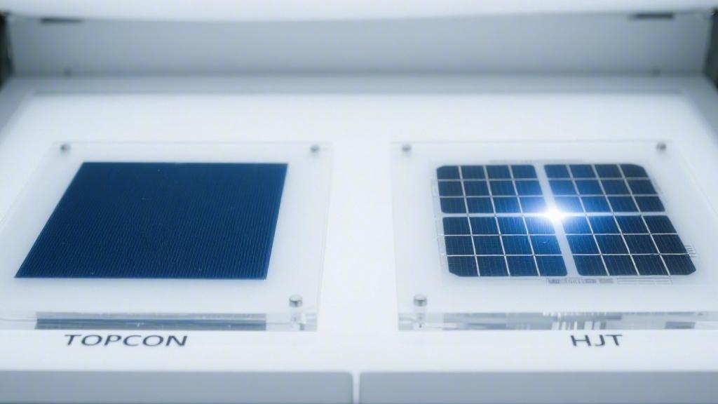
The printed width of front and rear grid lines for HJT cells is typically maintained at 30-32 micrometers. These extremely fine low-temperature silver paste lines control front-side shading losses to around 2.2%. In comparison, TOPCon cells must withstand high-temperature sintering, causing their silver-aluminum paste grid lines to spread outward during processing, with widths mostly at 45-50 micrometers, elevating their front-side shading loss to 3.4%.
HJT's low-temperature silver paste has excellent morphology retention ability, with grid line heights reaching 15 micrometers, which can reflect some lateral light back into the silicon wafer. TOPCon's grid lines tend to flatten after 800°C high temperatures, usually standing only 10 micrometers high. This morphological difference yields HJT an optical utilization rate at low illumination angles that is 0.3% higher than TOPCon.
l In the solar spectrum ranging from 300 nm to 1200 nm, the TCO film on the surface of the HJT cell demonstrates outstanding anti-reflective performance. Since the refractive index of TCO (Transparent Conductive Oxide) is about 2.0, falling exactly between glass (1.5) and the silicon wafer (3.8), it forms a natural optical gradient layer, reducing reflection loss to below 3%.
l Metallization Area: After adopting 0BB (busbarless) technology, HJT's metal coverage dropped from 3.5% to 0.6%, substantially freeing up the light-receiving area.
l Grid Distribution: Fine grid line spacing is set at 1.6 millimeters, striking a balance between resistance loss and optical shading while ensuring carrier collection efficiency.
l Reflection Path: The pyramid texture height on the surface of the silicon wafer is 3-5 micrometers. Coupled with the TCO layer, total internal reflections at the interface increase by 1.2 times.
Besides physical shading, TOPCon's rear 150-200 nanometer doped polysilicon layer creates severe parasitic absorption. When short-wave light with a wavelength less than 600 nm hits, the high-concentration phosphorus atoms in the polysilicon layer absorb the photons and convert them into heat rather than generating current. Experimental data shows this polysilicon layer causes a near 25% short-wave External Quantum Efficiency (EQE) loss on the rear side.
This parasitic absorption also exists in the long-wave band (1000 nm), manifesting as the Free Carrier Absorption (FCA) effect. Because TOPCon's rear polysilicon layer has a doping concentration higher than 10²⁰, about 1.5% of infrared photons dissipate before ever entering the silicon substrate. HJT completely avoids this issue; its intrinsic amorphous silicon thin film has a thickness of only 5-10 nanometers, making its photon interception effect almost negligible.
l The travel length of light within the cell depends on the internal reflectivity. The TCO film on both sides of the HJT cell possesses extremely high transmittance in the infrared band. Paired with a low-temperature paste offering a reflectivity above 95%, the effective optical path of photons within the silicon wafer increases by over 20%, translating directly into an enhancement of short-circuit current density.
l Absorption Coefficient: Amorphous silicon possesses an extremely low absorption coefficient in its wide bandgap state, making HJT's Internal Quantum Efficiency (IQE) at 400 nm approach 99%.
l Refractive Index Matching: The POE encapsulant film has a refractive index of 1.48, offering an optical coupling efficiency with the TCO layer that is about 0.5% higher than EVA.
l Surface Roughness: The textured silicon wafer surface broadens the distribution range of incident light angles. HJT's low-temperature process preserves the sharpness of the pyramid structures, enhancing light-trapping effects.
Optical loss also stems from material matching at the module level. HJT modules typically utilize high-transmittance, ultra-clear glass with an iron content below 100 ppm to guarantee energy output. In real-world operations, because HJT cells are more transparent, the escape rate of secondary reflected light received on their rear side is lower inside the cell. According to field measurements in high-irradiance Middle Eastern regions, HJT's optical gain remains stably 1.5 watts/m² higher than TOPCon's.
During the module encapsulation process, because HJT does not require high-temperature soldering, its internal light-receiving structure undergoes no thermal stress deformation. Conversely, the high temperatures during TOPCon string soldering can cause micro-cracks along the edges of the grid lines; these micrometer-scale physical defects induce diffuse reflection of incident light, resulting in about a 0.1% fluctuation in optical efficiency. HJT's flattened connection technology secures the physical stability of the light entrance path.
l In spectral response testing, HJT's External Quantum Efficiency (EQE) in the 300-500 nm band is about 8% higher than TOPCon's.
l Blue Light Response: The lack of a heavily doped region grants HJT a 2% higher generation efficiency than TOPCon between 7 AM and 9 AM.
l Angular Characteristics: At solar incident angles greater than 60 degrees, HJT's TCO film maintains better anti-reflective stability.
l Encapsulation Gain: The total optical transmittance under double-sided POE encapsulation reaches 91.5%, mitigating photon loss caused by interface refraction.
The control of optical losses is directly linked to the cell's current output. HJT's short-circuit current density (Jsc) can usually hit over 40.5 mA/cm². Although TOPCon excels in front-side passivation, restricted by its rear-side polysilicon absorption, its Jsc is often limited to around 39.2 mA/cm². The vast majority of this 1.3 mA/cm² gap originates from the optical differences brought about by the aforementioned microstructures.
Under prolonged ultraviolet light exposure, the extinction coefficient of TOPCon's polysilicon layer experiences a minor shift, causing its optical coupling performance to decline by about 0.05% annually. HJT's TCO layer belongs to inorganic oxide materials; after passing a 2000-hour UV aging test (UV150), its refractive index fluctuation is less than 0.01, securing long-term stable light capture capabilities.
The thermal expansion coefficient of HJT's low-temperature thin film system matches the silicon wafer more closely, leaving extremely few optical voids at the interface. Meanwhile, under alternating high and low temperatures, the interface between TOPCon's polysilicon and oxide layers might exhibit a microscopic tendency to delaminate, increasing total internal reflection loss and causing an additional 0.2% optical degradation in power generation after the third year of operation.