Thin-Film vs. Crystalline Silicon Photovoltaic Cells | Conversion Efficiency, Low-Light Performance
Crystalline silicon cells dominate with 15-22% conversion efficiency, ideal for maximizing power in limited spaces.
Thin-film excels in high-temperature and diffuse low-light conditions, offering more consistent dawn/dusk output but requires significantly more installation area for equivalent wattage.
Conversion Efficiency
The current photovoltaic market is dominated by crystalline silicon technology, accounting for over 90% of the share.
Its mass production efficiency is approaching the theoretical limit of 29.4%, with the mass production efficiency of N-type monocrystalline silicon generally reaching 24.5%-25.5%.
However, thin-film batteries are challenging with their unique technological paths.
The mass production efficiency of cadmium telluride modules is approaching 20%, while the laboratory efficiency of emerging perovskite technology has exceeded 26%, with the potential for tandem cells to reach over 33%.
Crystalline Silicon Cells
How are crystalline silicon cells manufactured?
The starting point for crystalline silicon cells is metallurgical grade silicon, refined from quartz sand.
It is then purified into solar-grade polysilicon via the Siemens process or a fluidized bed reactor, achieving a purity exceeding 99.9999% (six nines).
This silicon material is melted and then crystal growth occurs primarily through two main methods:
l Czochralski Method: This is the mainstream method for producing monocrystalline silicon. A seed crystal is dipped into molten silicon and slowly rotated and pulled upward, forming a cylindrical monocrystalline silicon ingot. The entire process requires precise control of temperature and pulling speed to ensure a complete lattice structure.
l Ingot Casting Method: Molten silicon is poured into a quartz crucible, and by controlling the cooling direction, it solidifies into a multicrystalline silicon ingot filled with different crystal grains. This process has lower costs, but grain boundaries exist between the crystals.
Currently, silicon wafer thickness has decreased from around 180 microns a decade ago to 150-160 microns, with even thinner wafers (below 130 microns) under development, aiming to reduce silicon material consumption.
P-type vs. N-type: The Fundamental Difference in Technology Paths
Silicon wafers themselves have poor conductivity and need to be doped with specific impurities to alter their electrical properties. This forms two basic technology paths:
1. P-type Silicon:
l Doping Element: Boron atoms are doped into the silicon, creating positively charged holes as the majority charge carriers.
l Mainstream Technology: PERC has been the absolute mainstay over the past decade. It deposits a passivation film on the back of the cell to reflect unabsorbed photons and prevent electron recombination at the rear, thereby improving efficiency.
l Efficiency and Challenges: Mass production efficiency is generally between 22%-22.5%. However, it is relatively sensitive to light-induced degradation, and its efficiency is approaching its theoretical ceiling of about 24.5%.
2. N-type Silicon:
l Doping Element: Phosphorus atoms are doped into the silicon, producing negatively charged electrons as the majority charge carriers.
l Advantages: Higher tolerance to impurities, virtually no light-induced degradation, and a theoretical efficiency limit far exceeding that of P-type.
Representative Technologies:
l TOPCon: A passivated contact technology that forms an ultra-thin layer of silicon oxide and doped polysilicon on the rear side of the cell, significantly reducing surface recombination. Current mass production efficiency is between 24.8%-25.5%, and it is the mainstream for current capacity expansion.
l HJT: Uses amorphous silicon thin films to form the PN junction. It has a symmetrical structure and low process temperature. Inherently possesses excellent temperature coefficient and bifaciality. Mass production efficiency is above 25%, but equipment and material costs (e.g., low-temperature silver paste) are higher.
l IBC: Moves all the front-side metal electrode gridlines to the rear side, leaving the front side completely unshaded, minimizing optical losses, and enabling very high efficiencies exceeding 26%.
Key Paths for Efficiency Improvement
Improving the efficiency of crystalline silicon cells is a "micron-level war" against energy losses, primarily focusing on the following aspects:
Optical Losses:
l Textured Surface: Anisotropic etching with an alkaline solution creates pyramid structures on the silicon wafer surface, enabling multiple reflections and trapping light within the cell.
l Anti-Reflection Coating: A silicon nitride film is deposited on the cell surface, utilizing interference effects to reduce surface reflection.
Electrical Losses:
l Passivation Technology: Such as the aforementioned PERC, TOPCon, etc. The core purpose is to reduce the recombination rate of charge carriers at the surface and within the bulk of the silicon wafer.
l Electrode Technology: Using finer metal gridlines (achieved through multi-busbar technology or screen printing) to reduce shading of sunlight.
Cost and Market Position
According to data from the International Energy Agency and the U.S. Department of Energy, the price of crystalline silicon modules has dropped from over $2/W in 2010 to around $0.10-$0.15/W currently.
Its market share has long remained above 95%, forming a complete globalized supply chain from polysilicon, wafers, and cells to modules.
Physical Limits and Challenges Faced
The efficiency improvement of crystalline silicon cells is facing the constraint of the Shockley-Queisser theoretical limit (approximately 29.4%).
The efficiency of the most advanced laboratory cells has reached 26.8%, very close to this ceiling. The main energy loss mechanisms include:
l Thermalization Loss: Photons with energy higher than the silicon bandgap lose their excess energy as heat.
l Transmission Loss: Photons with energy lower than the silicon bandgap cannot be absorbed.
l Recombination Loss: Generated electron-hole pairs recombine before being collected by the electrodes.
To break through the limit, the industry is focusing on tandem cell technology, particularly depositing perovskite cells on top of silicon cells to form a tandem structure.
This structure can utilize different materials to absorb different wavelengths of sunlight, with a theoretical efficiency limit exceeding 40%.
Thin-Film Cells
The fundamental difference between thin-film cells and crystalline silicon cells is that they do not require manufacturing a silicon ingot and then slicing it into wafers.
Instead, through a series of vapor deposition processes, a photovoltaic material layer only a few microns thick (about one-hundredth the thickness of a human hair) is directly grown onto a substrate such as glass, stainless steel, or polymer.
This manufacturing method determines its characteristics of being light, thin, and even flexible.
Main thin-film technology routes include cadmium telluride (CdTe), copper indium gallium selenide (CIGS), and perovskite.
The different light-absorbing materials used in each technology lead to significant differences in their performance, cost, and manufacturing processes.
Cadmium Telluride (CdTe): The Thin-Film Technology with the Largest Current Market Share
Cadmium Telluride is the core technology of the US company First Solar and is currently the most mature thin-film photovoltaic solution.
Material and Manufacturing: The core process involves sequentially depositing multiple thin films on a glass substrate to ultimately form a PN junction.
Efficiency Data:
l Champion laboratory cell efficiency: 22.3%
l Current mass production module efficiency: Approximately 19.0% - 20.5%
l The roadmap for the next 2-3 years indicates that mass production efficiency is expected to exceed 22%.
Cost and Sustainability: Its manufacturing steps are far fewer than for silicon, with lower energy consumption, giving it potential for lower costs. Regarding the toxicity of cadmium, the industry has established a complete recycling system through an "Extended Producer Responsibility" system, ensuring that over 95% of the materials can be recycled and reused after the module's end-of-life, with cadmium being stabilized and solidified in the glass, preventing environmental leakage.
Performance Characteristics: CdTe cells have excellent hot-spot performance and high resistance to damp heat. Their temperature coefficient is typically around -0.25%/°C, better than silicon's approximately -0.30%/°C, meaning their actual output power degrades less in hot environments.
Copper Indium Gallium Selenide (CIGS): A Technology with High Efficiency Potential
CIGS technology uses a compound semiconductor composed of four elements. By adjusting the gallium/indium ratio, its bandgap can be changed, optimizing absorption of the solar spectrum.
Material and Manufacturing Challenges: The manufacturing process for CIGS is very complex, requiring precise control of the stoichiometric ratio of the four elements and their uniformity on the substrate. Main deposition techniques include co-evaporation and sputtering followed by selenization. Process complexity is the main reason for its high cost.
Efficiency Data:
l Champion laboratory cell efficiency: 23.6%
l Mass production module efficiency: Typically between 16% - 19%, indicating a significant gap between lab and production line efficiency.
Application Characteristics: A significant advantage of CIGS technology is that it can be fabricated on flexible substrates (such as stainless steel foil, polyimide), making it very suitable for building-integrated photovoltaics (BIPV) and lightweight applications.
Perovskite: The Most Disruptive Emerging Force
Perovskite refers to a class of compounds with a specific crystal structure. Its photovoltaic materials (e.g., CH₃NH₃PbI₃) can be prepared via solution-based methods (similar to printing), which completely changes the manufacturing paradigm for solar cells.
l Revolutionary Manufacturing Process: Perovskites can be prepared using low-temperature solution-based methods like spin-coating, blade coating, and inkjet printing.
l Remarkable Efficiency Climb:
l The laboratory efficiency of single-junction perovskite cells has increased from 3.8% in 2009 to over 26.1% currently, a rate far exceeding any other photovoltaic technology.
l Its greatest potential lies in tandem cells. Perovskite cells absorb visible light well, and when combined with silicon cells that are good at absorbing infrared light, they form a "two-junction tandem cell" with a theoretical efficiency limit exceeding 40%.
l Core Challenge: Stability. Perovskite materials are sensitive to moisture, oxygen, and high temperatures. Long-term operational stability is the biggest obstacle to their commercialization. Currently, through material composition optimization and improved encapsulation technology, their stability has improved from initial hours to thousands of hours, but there is still a gap compared to the 25+ year lifespan guarantee of silicon cells.
Performance Advantages of Thin-Film Cells
Beyond efficiency data, thin-film cells exhibit some inherent advantages in actual power generation:
1. Low Temperature Coefficient: The power temperature coefficient (absolute value) of thin-film cells is generally lower than that of silicon cells. This means that when the module temperature rises from the standard test condition of 25°C to 50-60°C common in summer, the power loss of thin-film cells is smaller.
2. Better Low-Light Response: Thin-film materials typically have a narrower bandgap, leading to better absorption and response to diffuse light during early morning, evening, or cloudy days, potentially resulting in longer effective daily generation time.
3. Low Angular Loss: When the sun's angle of incidence is low, the power output decline of thin-film cells is less than that of silicon cells.
Cost Structure and Market Positioning
The production process for thin-film cells is highly integrated. A large glass substrate enters the production line and, after a series of deposition steps, outputs a complete module directly. This integrated process reduces intermediate steps, lowering material handling and energy consumption. Its main market positioning is in:
l Large-Scale Ground-Mounted Power Plants: Due to their low degradation and good high-temperature performance, they can be competitive in terms of Levelized Cost of Energy in hot, arid regions.
l Commercial and Industrial Rooftops: Lightweight modules impose lower load requirements on roofs.
l Building-Integrated Photovoltaics (BIPV): Especially flexible, customizable CIGS modules can be directly integrated into building facades or roofs.
Low-Light Performance
Under low-light intensity of 180-200 W/m² (less than 20% of STC), the open-circuit voltage degradation of cadmium telluride thin-film modules is about 5-8% lower than that of monocrystalline silicon. Furthermore, their absorption efficiency for blue-violet light (wavelength 450-500nm), which dominates on cloudy days, is over 10% higher than that of crystalline silicon.
The temperature coefficient further amplifies this difference—the power temperature coefficient of crystalline silicon is about -0.35%/°C, while for thin-film it is only -0.25%/°C. Under the same low-light and temperature rise conditions, the actual power output degradation of thin-film modules is slower.
Measured data indicates that in regions with an average annual irradiance below 1300 kWh/m², thin-film modules can generate 3-5% more annual energy yield compared to crystalline silicon modules of the same nominal power, thanks to their superior low-light response.
Evaluating Low-Light Performance
Metrics for Measuring Low-Light Performance
It is typically measured at two key points: 200 W/m² and 800 W/m².
Low-Light Performance Ratio: This ratio is calculated as (Pmax @ low irradiance / Pmax @ 1000 W/m²). A high-quality module should achieve an output power of 90% or more of its rated power at 200 W/m². For example, a comparative test of different technology modules showed that at 200 W/m², 25°C:
l An advanced cadmium telluride thin-film module output 92.5% of its rated power.
l An efficient PERC monocrystalline silicon module output 89.8% of its rated power.
l This represents an actual output difference of about 2.7 percentage points.
Core Quantitative Indicators
Beyond a single power ratio, the following parameters together form a complete picture for evaluating low-light performance:
1. Pmax Ratio at Low Irradiance: Testing institutions measure the module's power output at multiple irradiance levels between 200 W/m² and 1000 W/m².
2. Dynamic Change in Performance Ratio (PR): The Performance Ratio is the ratio of the system's actual output to its theoretical output. Under low-light conditions, the system's PR naturally decreases because fixed losses like inverter startup loss and line loss constitute a larger proportion of the total system power. However, modules with better low-light performance can partially offset this decline, allowing the system to maintain relatively high generation efficiency in the early morning and evening. Data analysis shows that during periods with irradiance below 400 W/m², systems using modules with excellent low-light performance can extend their daily effective generation time by about 45 minutes.
3. Spectral Response and Low-Light Performance: A material's quantum efficiency curve reveals its sensitivity to different light wavelengths. On cloudy days, the proportion of blue light in the sky's diffuse light increases. Modules with higher quantum efficiency for short-wavelength light (300-500 nm) have an inherent advantage in such environments. Laboratory data shows that the quantum efficiency of some thin-film modules at 450 nm wavelength is over 15% higher than that of standard silicon modules, directly translating into generation gains under diffuse light conditions.
Importance of the Test Environment
Laboratory data is fundamental, but real-world validation is equally crucial. Independent third-party testing agencies establish outdoor test fields in different climate zones for long-term monitoring. The data they collect can reveal the modules' low-light performance in real environments, for example:
l On a typical overcast autumn/winter day in Munich, Germany, with average irradiance around 300 W/m², monitoring found that the daily energy yield of thin-film modules was about 4% higher than that of crystalline silicon modules of the same nominal power.
l This advantage is more pronounced in cloudy climates like Seattle, USA, where the annual energy yield gain can reach 3-5%.
Power Generation Capability
The Importance of Voltage Under Low Light
When light intensity decreases, the current generated by a PV module decreases almost linearly, but the change in voltage is different. The open-circuit voltage has a logarithmic relationship with light intensity, decreasing much more slowly.
Therefore, under low-light conditions, a module that can maintain a higher voltage will have a higher output power.
Specific data shows that when irradiance drops from 1000 W/m² to 200 W/m², the short-circuit current of a typical monocrystalline silicon module drops to about 20% of its STC value, but its open-circuit voltage may only drop by 10-15%.
For example, a module with a Voc of 40V might still maintain a voltage above 35V at 200 W/m².
Different technologies have varying abilities to maintain voltage, with thin-film modules typically exhibiting a gentler voltage degradation curve.
Influence of Spectral Response
When sunlight passes through clouds, the direct light module decreases, and the proportion of diffuse light increases.
The spectral distribution of diffuse light is different from direct light, with a relatively higher proportion of short-wavelength blue-violet light.
The sensitivity of the module material to different light wavelengths (i.e., spectral response) directly affects its efficiency in capturing the energy of diffuse light.
Quantum efficiency maps show that thin-film materials like CdTe typically have 10-20% higher quantum efficiency in the 300-500 nm wavelength range compared to crystalline silicon.
Under cloudy conditions, thin-film modules can convert a greater proportion of incident photons into electricity.
Measured data indicates that under completely overcast conditions, the generation advantage of thin-film modules relative to crystalline silicon modules of the same power can reach 3-5%.
The Superimposed Effect of Temperature Coefficient
Low-light environments are often accompanied by lower operating temperatures, and lower temperatures enhance the performance of all types of modules.
However, because different technologies have different temperature coefficients, the extent of this enhancement also varies.
The following table compares typical power temperature coefficients of different technologies and their impact in low-light environments:
Technology Type | Power Temperature Coefficient | Power Degradation for 25°C to 35°C Temperature Rise | Performance in Low-Light and Fluctuating Temperature Environments |
Monocrystalline Silicon | -0.35%/°C | Approx. 3.5% | Output power fluctuates more noticeably with temperature changes |
Multicrystalline Silicon | -0.40%/°C | Approx. 4.0% | Poorer output stability |
Cadmium Telluride Thin-Film | -0.25%/°C | Approx. 2.5% | More stable output |
Quantitative Assessment Methods for Low-Light Performance
The IEC 61,853-1 standard specifies the method for measuring module performance at multiple irradiance levels between 200-1,000 W/m².
The industry typically focuses on the performance ratio at two specific points: 800 W/m² and 200 W/m²:
800 W/m² Ratio (%) = (Pmax @ 800 W/m² / Pmax @ 1000 W/m²) × 100%
200 W/m² Ratio (%) = (Pmax @ 200 W/m² / Pmax @ 1000 W/m²) × 100%
High-performance modules typically have an 800 W/m² ratio exceeding 95% and a 200 W/m² ratio exceeding 90%.
For example, test data for a certain brand of CdTe module shows its 200 W/m² ratio reaches 92.5%, while a high-efficiency monocrystalline silicon module achieves 89.3%.
Analysis of Actual Energy Yield Impact
Differences in low-light performance directly translate into differences in annual energy yield.
According to monitoring data from the US National Renewable Energy Laboratory in different climate zones:
In northern Germany, with an average annual irradiance of about 1000 kWh/m² and frequent cloudy weather, monitoring data shows that modules with excellent low-light performance yield 4-6% more annual energy than standard modules.
In the Arizona desert, USA, with an average annual irradiance exceeding 2200 kWh/m², dominated by direct light, the energy yield difference due to low-light performance narrows to 1-2%.
System Design Considerations
A module's low-light performance also influences system design choices. For modules with better low-light performance, it may be appropriate to consider:
l Using inverters with a lower startup voltage to extend daily generation time.
l Ensuring good output even in sites with some shading.
l Achieving better winter generation performance in higher latitude regions.
Thin-Film vs. Crystalline Silicon
Differences in Materials and Production Processes
Crystalline silicon cells use silicon material as the primary raw material.
After purification, the silicon is either pulled into ingots (monocrystalline) or cast into blocks (multicrystalline), then sliced into wafers.
These wafers undergo texturing, diffusion, etching, coating, and other processes to become cells, which are finally encapsulated into modules.
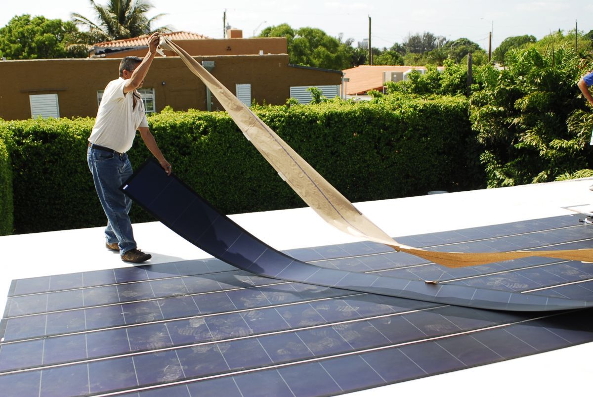
Thin-film cells are different. They are made by directly depositing photovoltaic material a few microns thick onto a substrate like glass, stainless steel, or polymer.
Mainstream technologies include Cadmium Telluride (CdTe), Copper Indium Gallium Selenide (CIGS), and Amorphous Silicon (a-Si).
This process is akin to "coating" the substrate, significantly reducing silicon material consumption.
Differences in Appearance and Physical Characteristics
These different manufacturing processes lead to distinct differences in product appearance and physical characteristics:
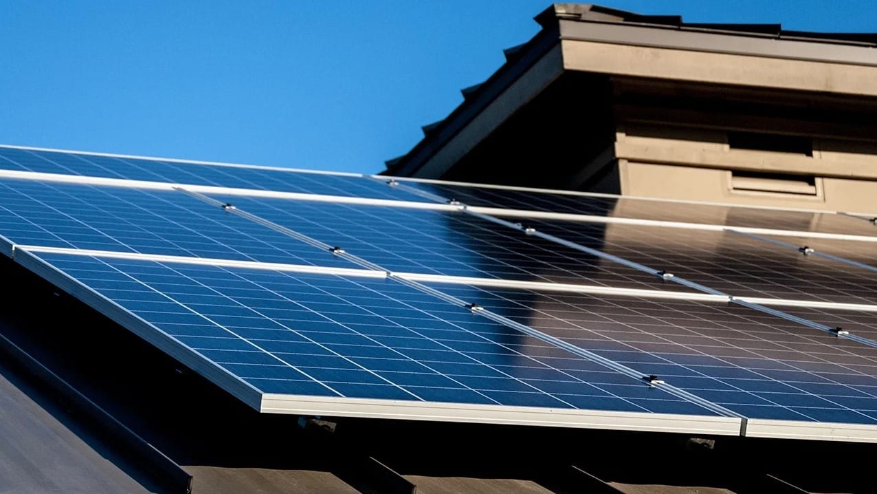
l Crystalline Silicon Modules: Typically consist of dark blue or black rectangular cells connected by gridlines, with a clear grid-like pattern on the surface.
l Thin-Film Modules: The surface is usually a uniform black or dark gray color, without obvious cell boundaries, giving a more integrated appearance. The modules can be made thinner, lighter, possess some flexibility, and can even be made semi-transparent or in custom shapes, facilitating building-integrated applications.
Historical Evolution of Conversion Efficiency and Cost
Crystalline silicon technology, especially monocrystalline silicon, has long held the lead in both laboratory and commercial module conversion efficiency records.
According to the latest reports, monocrystalline silicon laboratory efficiency exceeds 26%, with mainstream commercial module efficiency between 21%-23%.
Among thin-film technologies, CdTe and CIGS have champion laboratory efficiencies exceeding 22% and 24% respectively, while commercial module efficiencies are mostly in the 16%-20% range.
In terms of cost, crystalline silicon, benefiting from a massive industry scale and continuous technological optimization, has strong competitiveness in cost-per-watt.
The advantage of thin-film technology lies in its potential for low material consumption and a more simplified integrated production process, but under the current market scale, this cost advantage has not yet fully materialized.
Impact of Temperature Coefficient on Energy Yield
The temperature coefficient is a key parameter affecting actual generation performance, indicating the rate at which output power decreases as temperature increases.
l The typical power temperature coefficient for crystalline silicon modules is approximately -0.35%/°C to -0.45%/°C.
l The typical power temperature coefficient for cadmium telluride thin-film modules is approximately -0.20%/°C to -0.25%/°C.
This means that in the same high-temperature environment (e.g., a summer afternoon with module surface temperatures exceeding 60°C), the output power degradation of thin-film modules is significantly less than that of crystalline silicon modules.
In hot regions, this characteristic can translate into higher actual energy yield.
Performance Under Low-Light Conditions
Under low-light conditions such as early morning, evening, or cloudy days, thin-film modules typically demonstrate better power generation capability.
This is mainly due to their superior spectral response characteristics (better absorption of diffuse light) and higher ability to maintain open-circuit voltage.
Measured data shows that at 200 W/m² low light, the relative output power (relative to their nominal power) of some thin-film modules can be 2-3 percentage points higher than that of crystalline silicon modules.
This can give them an advantage in total annual energy yield in regions with frequent overcast/rainy climates.
The following table summarizes some typical characteristics of the two technologies:
Characteristic | Crystalline Silicon Module | Thin-Film Module (e.g., CdTe) |
Commercial Module Efficiency | 19% - 23%+ | 16% - 20%+ |
Power Temperature Coefficient | ≈ -0.35% / °C | ≈ -0.25% / C |
Low-Light Performance (200W/m²) | Relative output ~88-91% | Relative output ~90-93% |
Appearance | Dark blue, with gridlines | Uniform black, no gridlines |
Weight & Flexibility | Heavier, rigid | Lighter, some flexibility |
Application Scenario Selection
Different characteristics make them suitable for different application scenarios:
l For large-scale ground-mounted power plants, especially in areas with low land costs and abundant sunlight, high-efficiency and low-cost crystalline silicon modules are usually the preferred choice.
l For high-temperature regions, rooftop distributed projects, building-integrated projects requiring esthetics and light weight, and regions where low-light generation performance is valued, the advantages of thin-film modules may be more pronounced.