What is Polysilicon Used for in Solar
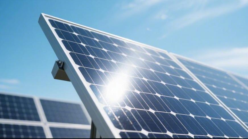
Polysilicon is the core raw material for manufacturing photovoltaic cells; after being purified to 99.9999%, it is cut into silicon wafers approximately 150 microns thick.
It generates electric current by absorbing photons, with a photoelectric conversion efficiency of about 20%, supporting the manufacturing of over 90% of solar panels globally.

Efficiency
Conversion Rate
The physical environment strictly mandated by Standard Test Conditions (STC) includes a fixed solar irradiance of 1000 watts per square meter, an air mass spectral parameter of AM1.5, and a constant test temperature of 25 degrees Celsius.
Inside such a rigorous laboratory temperature-controlled chamber, the photoelectric conversion values of mass-produced polysilicon solar cells typically fluctuate within a physical range of 19.5% to 20.8%.
The internal crystal structure of polysilicon contains grain boundary defect recombination centers on the order of 10^13 to 10^15 per cubic centimeter. When visible photons in the wavelength range of 380 to 780 nanometers strike the 160-micron-thick surface of the silicon wafer, approximately 12% to 15% of the light energy is converted into useless heat dissipation in the grain boundary regions.
To compensate for physical losses at the microscopic level, factories generally adopt the Plasma-Enhanced Chemical Vapor Deposition (PECVD) process on the light-receiving surface of the solar cells:
l Depositing an anti-reflection coating of silicon nitride with a thickness precisely maintained between 75 nanometers and 85 nanometers.
l Accurately anchoring the refractive index value at 2.05 at a wavelength of 600 nanometers.
l Forcibly suppressing the original 30% natural light reflectance of the bare silicon wafer surface to below the safe line of 6%.
The Back Surface Field (BSF) process utilizes screen printing equipment to coat the back of the silicon wafer with aluminum paste with a thickness of 20 to 30 microns.
After undergoing extreme rapid sintering for 2 minutes in a high-temperature conveyor furnace at 800 degrees Celsius, the effective surface recombination velocity of minority carriers is strictly limited to below 200 cm/s, rigidly pulling up the overall conversion value of the cell by 0.4 percentage points.
Does Power Drop Slowly?
During the first 24 months of grid-connected operation, polysilicon modules must endure a physical power decline caused by Light-Induced Degradation (LID). In the ingot casting process, the concentration of oxygen atoms dissolved in the liquid silicon is perennially maintained at 5×10^17 per cubic centimeter, which is a full order of magnitude lower than that of the monocrystalline Czochralski process.
Boron-oxygen complexes deactivate after being continuously exposed to 1000 hours of natural ultraviolet radiation, forcing the rated output power of the polysilicon module to drop by 2% to 2.5% in the first year.
From the 24th month of operation through to the 300th month, the linear annualized degradation rate of the module remains stable at an extremely low amplitude of 0.55% to 0.65% for many years. To cope with the Potential Induced Degradation (PID) leakage current phenomenon erupting in high DC voltage systems of 1000 volts or 1500 volts, assembly workshops heavily infuse POE encapsulant films with a volume resistivity exceeding 10^14 ohm·cm to replace traditional EVA materials.
Placed into an extreme testing aging chamber with an ambient temperature of 85 degrees Celsius and a relative humidity of 85% for continuous baking for 192 hours, the absolute power loss rate of polysilicon modules is controlled within the industry passing mark of 5%, ensuring that they still output 90% of their initial nominal electricity in their 25th year of service.
Afraid of the Heat?
The power temperature coefficient of a polysilicon solar cell is an engineering parameter that is always negative, and the average median of current mass production data fluctuates between -0.38%/℃ and -0.42%/℃.
According to the factory calibration standard of 25 degrees Celsius, when extreme noon sun exposure in a tropical desert climate causes the physical temperature of the module's backsheet to climb to 65 degrees Celsius, the temperature difference widens to 40 degrees Celsius.
Subjected to the physical penalty of the temperature coefficient, a polysilicon module with a factory nameplate rating of 300 watts will suffer a power discount of 15.2% to 16.8%, and its real-time peak output power will slip into the range of 250 watts to 254 watts.
To improve thermodynamic performance in high-temperature environments, the spacing of the heat sink fins installed on the back side of the aluminum alloy frame is widened to 45 mm to 55 mm.
l Relying on aerodynamic natural air cooling, an outdoor wind speed of 3 meters/second can strip away 3 to 5 degrees Celsius of localized accumulated heat from the backsheet.
l The surface sheet resistance value of phosphorus atoms inside the silicon wafer is adjusted upwards to 90 ohms/square to 110 ohms/square.
l Heavy doping methods reduce the reverse drift rate of dark current in the PN junction by 11% in high-temperature environments.
l This successfully recovers 1.2 watts of absolute power loss in a 70-degree Celsius environmental chamber.
Generating Power on Cloudy Days
At dawn, at dusk, and on rainy days with heavy cloud accumulation, the vertical radiation intensity reaching the ground will plummet steeply from the standard value of 1,000 W/m² to 200 W/m², or even break through the 100 W/m² bottom line.
Within the short to medium wavelength spectral band of 400 nm to 600 nm, polysilicon materials still retain an Internal Quantum Efficiency (IQE) of 85% to 92%.
When ambient illuminance shrinks to the low irradiance threshold of 200 W/m², the series resistance (Rs) of the polysilicon cell expands from 0.003 ohms to 0.015 ohms, while the shunt resistance (Rsh) is maintained above 800 ohms, suppressing the leakage current to below 0.1 amps.
Changes in the underlying resistance network allow the module's relative conversion efficiency under low illumination to remain robustly in the 95% to 97% range of its full-load rated efficiency at 25 degrees Celsius.
About 45 minutes after sunrise, when the light intensity climbs past the minimum startup threshold of 80 W/m², the accompanying microinverter for the polysilicon immediately establishes a 120-volt DC startup voltage and begins delivering an initial grid-tied current of 0.5 amps to the main grid.
Factory Yield Rate
The sixth-generation directional solidification casting furnace with a loading capacity of 1200 kilograms completes a full thermodynamic cycle—including heating, melting, crystal growth, and cooling—locked into a rigid timeframe of 52 to 56 hours, with power consumption sharply reduced from 12 kWh/kg a decade ago to 6.5 kWh/kg.
The slicing workshop fires up fine-pitch diamond wire saws with a linear speed of 1500 meters/minute, consuming 110 minutes to simultaneously slice 2500 finished silicon wafers, each 160 microns thick, from a 400-millimeter-long square silicon ingot.
The rates of physical mechanical breakage and micro-cracking on the edges along the conveyor belt are locked below 0.2% by high-speed machine vision rejection systems capturing 60 frames per second. The fully automatic cell printing and sintering assembly line has a fixed hourly throughput of 6,000 to 7,200 pieces, extruding ultra-fine silver grid lines with a width of only 25 to 30 microns through the mesh screen.
For every 1 gram of 99.9% purity front-side conductive silver paste consumed, the Fill Factor (FF) of the solar cell is pushed up and stabilized in the 79.5% to 81.2% range. The comprehensive detection rate for first-class products on the fully automated production line perennially remains above the 98.5% baseline.
Environmental
Is Electricity Consumption High?
The fundamental physical process of producing polysilicon is accompanied by extremely high-intensity grid loads. Heating quartz sand in an electric arc furnace to 1900 degrees Celsius for carbon reduction reactions to obtain metallurgical grade silicon strictly binds 12,000 to 13,000 kilowatt-hours of electrical energy consumption per ton produced.
When 99% purity crude silicon is fed into the fully enclosed reduction furnace of the modified Siemens process, within a constant temperature vapor deposition zone of 1,050 to 1,100 degrees Celsius, trichlorosilane gas is reduced into polysilicon rods with a purity of 99.9999%.
During the long crystal growth cycle of 50 to 60 hours, the water-cooling jacket on the outer wall of the furnace must rely on industrial cooling water flowing at 500 to 600 cubic meters per hour to carry away a massive amount of thermal energy.
The precipitation of every kilogram of photovoltaic-grade polysilicon is accompanied by a massive electricity consumption of 45 kWh to 55 kWh. Granular silicon production lines utilizing Fluidized Bed Reactor (FBR) technology forcefully suppress the electrical energy loss per kilogram of polysilicon into the 15 kWh to 18 kWh range by blowing silane gas into the furnace and maintaining a medium-low temperature suspension reaction environment of 650 to 700 degrees Celsius.
"In the thermodynamic conversion process of vapor deposition, over 65 percent of the electrical energy input into the reduction furnace is converted into unusable waste heat and dissipated, causing the basic monthly electricity bill of traditional polysilicon factories to frequently breach the 5 million dollar budget red line."
Are the Exhaust Gases Toxic?
On the chemical purification assembly line converting industrial silicon into high-purity polysilicon, hydrogen chloride (HCl), trichlorosilane (SiHCl3), and the byproduct silicon tetrachloride (SiCl4) are listed as hazardous compounds that must be strictly locked down.
In a standard Siemens process reactor, for every 1 kilogram of pure polysilicon produced, the reaction byproducts inevitably contain 10 to 15 kilograms of liquid-flowing silicon tetrachloride. Modern purification factory workshops are mandatorily equipped with cold hydrogenation reaction towers featuring pressure parameters reaching 1.5 to 2.5 megapascals and operating temperatures maintained at 500 to 600 degrees Celsius.
The collected liquid silicon tetrachloride undergoes a violent gas-liquid-solid three-phase mixing reaction with hydrogen and silicon powder inside the tower, reversely generating trichlorosilane, which holds industrial recycling value.
The end of the exhaust pipeline is connected to a three-stage alkaline spray scrubber containing a 15% to 20% sodium hydroxide (NaOH) solution, which neutralizes and cleans the escaped residual hydrogen chloride gas at a flow rate of 200 to 250 liters per minute.
The pH value of the scrubbed industrial wastewater is strictly tested and neutralized to a safe neutral standard of 6.5 to 8.5 before it is permitted to be discharged into sewage treatment pools for 48 hours of static sedimentation.
"The full-coverage integration of closed-loop cold hydrogenation piping systems forcibly pins the chemical reverse conversion and recovery rate of highly toxic silicon tetrachloride at the physical boundary of 99.5 percent, cutting off the pathway for chlorine-containing compounds to escape into the outdoor atmosphere."
Calculating the Carbon Footprint
Manufacturing a conventional polysilicon solar panel with a rated output power of 300 watts—from upstream silica sand mining, electric arc furnace smelting and purification, diamond wire slicing, texturing and diffusion, to final encapsulation and factory dispatch—cumulatively releases about 350 to 400 kilograms of carbon dioxide equivalent into the atmosphere across the entire industry chain.
Assuming this photovoltaic module is installed flat in a dry, sunny area at 35 degrees North latitude with an average annual total solar radiation of 1500 kWh/m², during its 1st to 5th years of standard operation, it can steadily deliver about 420 to 450 kWh of clean DC electricity to the main grid annually.
Compared to traditional coal-fired power generation units, which produce about 2.46 tons of carbon dioxide for every ton of standard coal burned, the carbon emission reductions achieved by this PV module replacing fossil fuels will reach a volume of 25 to 30 kilograms by its 30th day of operation.
Relying on continuous grid-connected operation with a normal uptime of up to 98%, the energy consumption during the polysilicon module's manufacturing cycle and the total greenhouse gases emitted early on are precisely offset within an Energy Payback Time (EPBT) of 1.2 to 1.5 years.
"Over the 25-year rated physical service lifecycle of a polysilicon photovoltaic module, the comprehensive greenhouse gas emissions produced during its early production stages account for only 5 to 7 percent of its total lifetime equivalent emission reductions from delivering clean electricity."
End-of-Life Dismantling
After a standard polysilicon solar panel weighing 19 kilograms is scrapped and retired, its physical composition contains 14 kilograms of ultra-clear low-iron tempered glass, 2 kilograms of aluminum alloy metal frame, 1.5 kilograms of high-molecular polymer backsheet, and approximately 0.8 to 1 kilogram of fragmented polysilicon materials.
The recycling processing line first uses a CNC mechanical dismantling bed to strip the aluminum alloy outer frame from the edges, and then pushes the remaining photovoltaic panel flat into a high-temperature pyrolysis rotary kiln pre-set to a temperature of 500 to 600 degrees Celsius.
After enduring 45 to 60 minutes of oxygen-free baking, the internal ethylene-vinyl acetate (EVA) encapsulant film used for bonding and sealing is completely carbonized and decomposed into volatile gases.
The surviving silicon wafer fragments are collected and immersed in a mixed solution of 60% nitric acid and 40% hydrofluoric acid. Following 12 continuous hours of acid leaching reactions, the conductive silver paste attached to the front and the aluminum grid on the back of the silicon wafers are completely dissolved.
A sodium chloride reagent is then added to the precipitation filtration pool for ion displacement extraction, which can displace 12 to 15 grams of industrial silver hidden within a single scrap panel. The overall chemical recovery purity of the silver reaches the 99.9% standard trading specification.
Sustainability
Is There Enough Sand?
Approximately 27.7% of the physical weight of the Earth's crust is occupied by the element silicon.
Mining high-quality quartz ore with a grade of over 99.5% serves as the initial material source for synthesizing polysilicon.
A photovoltaic-grade polysilicon purification production line with an annual capacity of 50,000 tons needs to process roughly 120,000 to 150,000 tons of raw silica ore per year.
Currently, the global annual mining volume of industrial quartz sand remains stable in the range of 50 million to 60 million tons, and the consumption for photovoltaic polysilicon accounts for less than 3% of the total output.
Over the past decade, the diameter of the diamond wire in the slicing workshop has shrunk from 0.12 millimeters to 0.05 millimeters.
Extremely fine cutting wires, paired with an equipment operating linear speed of 1500 meters/minute, have forcibly pushed the physical kerf loss rate during the cutting process down by 22%.
The raw silicon material consumption per watt of polysilicon PV module has plummeted from an initial 4.5 grams to between 2.6 and 2.8 grams.
Today, one kilogram of 99.9999% pure polysilicon ingot can reliably yield 55 to 62 standard-sized wafers with a thickness of 160 microns.
As ultra-thin 130-micron silicon wafers enter the workshop trial production phase, the megawatt capacity of module shipments corresponding to every 10,000 tons of polysilicon material is expected to increase by another 15% to 18% next year.
Clear Payback Calculation
The Energy Payback Time (EPBT) benchmarks the length of operation time required for a photovoltaic module to self-repay its manufacturing energy consumption.
From quartz sand smelting to final factory assembly, a 60-cell polysilicon panel with a rated output power of 280 watts cumulatively consumes about 220 to 250 kilowatt-hours of electrical energy at the manufacturing end over its entire lifecycle.
Laid flat in a dry desert area with an average annual total solar radiation of 1800 kWh/m² and configured with fixed metal brackets tilted at 30 degrees.
After filtering out line losses and inverter conversion losses, it provides an average of 5.5 effective full-load generation hours daily, capable of delivering 380 to 410 kWh of AC electricity to the local main grid over a full year.
By operating continuously outdoors for 0.8 to 1.1 years, the panel can 100% offset the sum of all thermal and electrical energy invested in the preliminary purification and processing procedures.
Throughout its subsequent 24-year conventional service life span, its Energy Return on Investment (EROI) will utterly soar to between 25 and 30 times the initial input volume.
Whenever the photoelectric conversion efficiency of a single polysilicon cell climbs upward by 0.5 absolute percentage points, the Energy Payback Time of the entire module can continue to be shortened by approximately 0.08 years.
Not Afraid of Time
The standard physical degradation warranty agreements provided by the factory for photovoltaic modules mandatorily cover a time span of 25 to 30 years.
The minority carrier lifetime within the polysilicon crystal lattice is typically maintained in an extremely short physical range of 10 to 30 microseconds.
Exposed to long-term irradiation by outdoor natural ultraviolet light with a wavelength of 280 nm to 400 nm, the light transmittance of the Polyolefin Elastomer (POE) encapsulant film experiences an average minor drop of 0.15% to 0.2% per year.
Superimposed with the light-induced degradation reaction of boron-oxygen complexes inside the silicon wafer, the peak output power loss in the first year is strictly confined within the physical red line of 2.5%.
Counting from the 13th month of operation all the way to the 300th month, the annualized power degradation rate of the panel is anchored for years within the extremely narrow band of 0.55% to 0.65%.
When a polysilicon module with a factory nameplate-rated power of 300 watts has served 25 full years weathering the elements in the field.
If removed and placed in a standard illumination test temperature-controlled chamber at 1,000 W/m², it can still measure an actual peak power output exceeding 242 to 248 watts.
The 6063-T5 anodized aluminum alloy profiles used for the physical frame maintain a yield strength above 110 megapascals year-round, calmly withstanding up to 210,000 hours of outdoor wind and sand friction as well as salt spray oxidative corrosion.