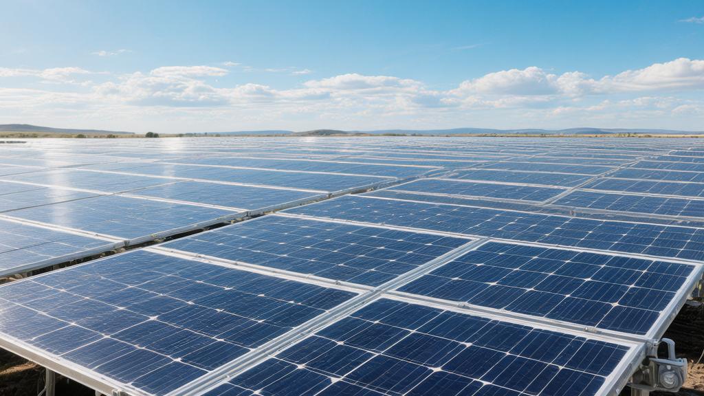
Are solar panels completely environmentally friendly?
Solar panels are not "completely environmentally friendly." They produce nearly zero emissions during power generation, but the mining of silicon, silver, aluminum, and the manufacturing processes consume energy and generate carbon emissions;
However, research shows that photovoltaic systems usually recover the energy consumed during manufacturing in about 0.5 to 1.2 years, and can "pay back" their carbon emissions within an average of about 2 years.
The bigger challenge lies at the end-of-life stage: global photovoltaic waste may reach 78 million tons by 2050, so whether a high-efficiency recycling system is established will determine just how eco-friendly it truly is.
The Carbon Payback Period
Calculating the Payback
Manufacturing a standard monocrystalline silicon photovoltaic module with a nominal peak power of 400 Watts consumes about 300 kWh of electrical energy throughout the entire production line process.
If the regional power grid where the manufacturing plant is located has a carbon emission intensity of 400 grams of CO2 equivalent per kWh, the module leaves the factory with an initial carbon debt of 120 kg.
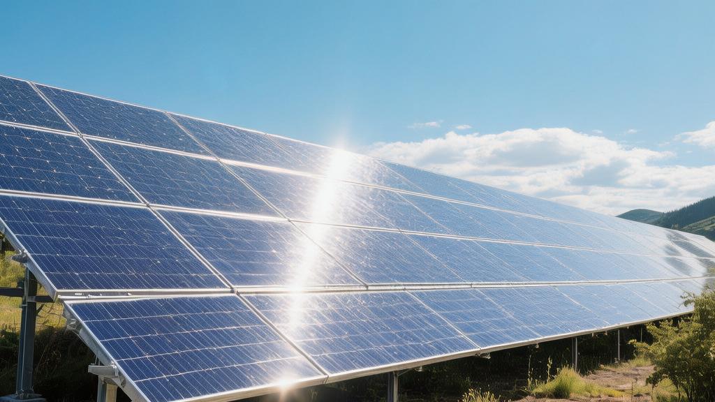
Installing this panel, with an area of about 1.9 square meters, at a 20-degree tilt on a roof in a region with an average peak sunshine time of 5 hours, produces about 1.8 kWh of AC power daily.
Assuming the local municipal grid relies on coal-fired power with carbon emissions reaching 800 grams per kWh, the panel running at full load can reduce greenhouse gas emissions by 1.44 kg per day.
By dividing the total carbon debt of 120 kg from the manufacturing period by the daily emission reduction yield of 1.44 kg, the system's carbon emission payback period falls precisely at 83.3 days.
If the same equipment is moved to Berlin, where the total annual radiation is 900 kWh per kWp, its carbon payback time extends to approximately 1.4 years.
Energy Consumption in Silicon Smelting
Purifying industrial silicon with 99% purity to 99.9999% polysilicon material consumes 50 to 60 kWh per kg in a reaction furnace at 1100°C.
A module containing 60 cells contains approximately 1.2 kg of high-purity silicon material, accumulating about 70 kWh of energy consumption in the purification stage.
Placing polysilicon in a quartz crucible to pull it into monocrystalline silicon rods at a high temperature of 1500°C takes a growth cycle of 72 hours per rod, adding 25 kWh of energy consumption per single module.
Slicing machines use diamond wires with a diameter of 50 microns to cut the silicon rods into wafers with a thickness of 130 microns, with the cutting process generating a 15% silicon mud loss rate.
From the mining of quartz sand raw materials to obtaining photovoltaic-grade silicon wafers, the energy conversion efficiency of the material transformation stage maintains an average of 65%.
The 65% conversion rate makes the carbon emissions from the silicon-based material processing stage account for 60% to 70% of the total carbon footprint of the solar panel's entire lifecycle.
Light Intensity Variance
In the Nevada desert, where the total average annual solar radiation is 2000 kWh per square meter, a 10 kW residential rooftop power station reaches the energy investment break-even point in 9.5 months.
Shipping 10 sets of the same photovoltaic equipment with a total weight of 200 kg to London for installation, where the average annual sunshine drops to 1000 kWh per square meter, extends the energy payback period to 19 months.
If the equipment is connected to a natural gas-dominated grid with a carbon emission factor of 200 grams per kWh, the emission reduction yield from replacing high-carbon energy decreases by 75%, and the carbon payback period increases to over 36 months.
Assuming the physical degradation lifespan of the system is 25 years, the Nevada sample achieves a 3,100% Energy Return on Investment (EROI) over a 300-month service period.
In a temperate maritime climate zone with a cloud cover as high as 60%, the same equipment produces a net energy gain of 1,500% at the end of its 25-year lifecycle.
Calculated at a linear power attenuation rate of 0.55% per year, the panel maintains a power output in its 25th year of service at 86.2% of the initial nominal power from the first year.
Glass and Aluminum Frames
The 3.2 mm thick photovoltaic patterned glass covering the solar cells accounts for 70% of the module's total weight of 20 kg.
Melting quartz sand in a glass kiln at 1500°C to produce tempered panels with a light transmittance of 91% generates approximately 16 kg of CO2 equivalent.
The anodized aluminum alloy frame that fixes the perimeter of the module weighs about 2.8 kg; the electrolytic aluminum process consumes 13.5 kWh of electricity per 1 kg of primary aluminum refined.
The 2.8 kg of frame material adds a power budget of 37.8 kWh, resulting in a carbon debt of 17 kg based on the global average grid carbon intensity.
The string inverter responsible for converting DC to AC has an average conversion efficiency of 98.5%, and its internal electrolytic capacitors have an expected lifespan of 10 to 15 years.
Performing 1.5 inverter hardware replacements over a 30-year system operation cycle adds 150 kg of carbon emissions to the system's full lifecycle, along with 600 USD in maintenance costs.
Production Line Acceleration
Production lines using 210 mm large-size silicon wafers can increase the peak power of a single module from 350 Watts to 600 Watts while maintaining the thickness of the frame aluminum.
Over the past 14 years, three significant process upgrade indicators have appeared in the photovoltaic industry:
· Between 2010 and 2024, the thickness of silicon wafers decreased from 180 microns to 130 microns; the 50-micron physical thickness reduction led to a 38% decrease in silicon material consumption per Watt.
· The average photoelectric conversion efficiency of cell cells has climbed from 16% with older rear-side technology to mass production exceeding 24% with new oxide layer structures.
· A 50% increase in relative power density has seen output jump from 180 Watts per square meter to 220 Watts, diluting manufacturing carbon emissions per unit area by 18%.
40% of global large-scale manufacturing plants have signed 100% renewable energy power purchase agreements, and the carbon footprint per Watt at the factory gate has dropped by 45% over the past five years.
Combining the statistical data of five ten-year technical variables, the median global carbon emission payback for solar modules has shortened from 2.8 years in 2015 to 1.1 years in 2024.
The Mining and Manufacturing Footprint
Mining
Producing 1 MW of installed capacity of solar panels requires mining approximately 10 tons of high-purity quartz sand ore.
Excavating deposits up to 50 meters deep in open-pit mines, for every 1 ton of raw silica ore with a grade above 99.5% extracted, heavy machinery driven by diesel emits about 15 kg of greenhouse gases.
The mining process is accompanied by heavy groundwater consumption, with an average of 1200 liters of fresh water consumed per ton of raw ore washed and crushed.
The environmental pressure from silver mining is also explicitly present; manufacturing a single panel with a nominal power of 400 Watts requires approximately 20 grams of silver.
Based on sample data from conventional silver mines in Mexico and Peru, extracting 1 gram of industrial silver with 99.9% purity requires processing 2.5 kg of waste residue containing heavy metals and using 0.8 liters of chemical solvent with a 0.5% cyanide concentration in the flotation process.
Silicon Purification
Smelters that convert raw ore into photovoltaic-grade polysilicon place quartz sand and carbonaceous reducing agents into an electric arc furnace to reduce industrial silicon to a purity of 98% to 99% at a temperature of 1900°C.
The reduction process consumes 14 kWh of electrical energy for every 1 kg of industrial silicon produced.
Subsequently, in the modified Siemens process, industrial silicon and hydrogen chloride gas generate trichlorosilane in a fluidized bed reactor at 300°C.
In a reduction furnace at temperatures as high as 1150°C, a 72-hour vapor deposition process allows trichlorosilane to grow on a silicon core into a polysilicon rod with a purity of 99.9999%.
In this chemical conversion stage, the electricity consumption per kg of purification fluctuates between 45 kWh and 50 kWh.
A polysilicon manufacturing plant with an annual capacity of 50,000 tons has an annual power consumption of 2.5 billion kWh at full load. If the local power grid is 60% dependent on coal-fired power, the polysilicon purification stage alone adds 1.5 million tons of CO2 equivalent to the atmosphere annually.
Slicing Wafers
Polysilicon material is placed in a quartz crucible and pulled into monocrystalline silicon rods at a high temperature of 1500°C, then sent to a slicing machine for processing.
Using diamond wires with a diameter of 40 to 50 microns running at a speed of 15 to 20 meters per second, the monocrystalline silicon rods are cut into square wafers with a standard thickness of 130 microns.
The slicing equipment consumes 1000 liters of coolant containing polyethylene glycol per hour to reduce friction temperatures and carry away chips.
The 130-micron thickness process standard is accompanied by a physical loss rate of about 15% in silicon mud; this powdered silicon material is extremely difficult to secondary purify or recycle.
A production line with a daily output of 1 million silicon wafers generates 3 to 5 tons of industrial wastewater containing trace metal powders and organic solvents every day. The wastewater treatment system requires an investment of 500,000 USD in environmental protection equipment and consumes a large amount of flocculants to reduce its Chemical Oxygen Demand (COD) to below 500 mg per liter for compliant discharge.
Coating
Bare silicon wafers are sent to a cleanroom and enter a chemical etching tank using a mixed solution of 2% to 5% hydrofluoric acid and nitric acid for surface texturing.
Treating every 1000 wafers of 210 mm size consumes 2.5 liters of hydrofluoric acid, forming a micron-level pyramid textured structure that pushes the sunlight reflectance on the silicon surface down from 30% to below 10%.
In the screen-printing process, automated robotic arms precisely apply conductive silver paste containing silver powder, glass powder, and organic solvents to the front and back of the silicon wafer. Each wafer consumes 100 mg to 130 mg of silver paste, which is then quickly baked in a sintering furnace at 800°C for 3 to 5 minutes to form the conductive circuit.
To connect 60 to 72 cells into a module, a welding machine uses tin-lead alloy solder ribbons with a melting point of 180°C to 190°C for physical connection.
Traditional Sn60Pb40 formula solder ribbons contain 40% lead; a 20 kg module contains approximately 12 to 15 grams of metallic lead.
The End-of-Life Crisis
End of Lifespan
Statistical models from the International Renewable Energy Agency (IRENA) predict that the cumulative weight of decommissioned photovoltaic modules globally will reach 78 million tons by 2050.
Based on a weight of 20 kg per panel with a nominal power of 400 Watts, a physical volume of 78 million tons is equivalent to 39 billion discarded modules.
The physical design lifespan of crystalline silicon panels is set within a range of 25 to 30 years.
After 300 months of high-intensity outdoor operation, the average photoelectric conversion efficiency attenuation rate touches the 80% threshold for decommissioning.
Based on a sample of 150 MW of early photovoltaic power plants installed in California in 2000, the actual output power in the 24th year dropped to 76.5% of the factory-rated parameters.
A physical hardware failure rate that increases by 5% annually sends a large number of first-generation power generation units into the waste treatment cycle 3 to 5 years ahead of schedule.
Transportation Costs are Too High
Transporting one ton of used panels from a residential roof to a specialized treatment plant 500 km away costs an average logistics range of 80 USD to 120 USD per trip.
Sending them to a municipal landfill within 50 km for burial compresses the disposal budget to 20 USD to 30 USD per ton.
The Waste Electrical and Electronic Equipment (WEEE) Directive enforced in Europe requires that the overall material recycling rate for photovoltaic modules must reach the legal compliance line of 85%.
The comprehensive recycling cost for 1 ton of used crystalline silicon modules falls within the statistical range of 350 USD to 400 USD.
The selling price of reclaimed materials in the commodity delivery market peaks at only 45 USD per ton.
A negative balance of up to 300 USD prevents 90.5% of recycling projects from achieving a commercial-grade return on investment.
Tearing Open the Film
The 0.5 mm thick ethylene vinyl acetate (EVA) polymer inside the panel has a cross-linking degree of up to 80%, tightly bonding the glass and silicon wafer with a strong adhesion of 1500 Newtons.
Using a pyrolysis furnace at 500°C to 600°C to burn 1 ton of used panels consumes 250 kWh of industrial electricity.
The concentration of volatile organic compounds released from the pyrolysis furnace chimney often breaks the safe emission upper limit of 100 mg per cubic meter.
Using the chemical solvent dissolution method to degrade the internal polymers involves soaking in a trichloroethylene solution in a constant-temperature reaction tank at 90°C for up to 120 minutes.
A single complete dissolution of 100 old panels of 1.7 square meters consumes 400 liters of 99% pure liquid organic solvent.
The purification costs for high-concentration waste liquid account for 45.5% of the total cost budget for the entire film-stripping process.
Extracted Material Category | Module Weight Percentage (%) | Current Process Average Recovery Rate | Refined Substance Purity Parameter | Recycling Market Unit Price (USD/kg) |
Patterned Tempered Glass | 70.0% | 65.5% | 95.0% | 0.015 |
Anodized Aluminum Frame | 18.0% | 98.0% | 99.0% | 1.850 |
Crystalline Silicon Cell Fragments | 4.0% | 45.0% | 90.0% | 0.450 |
Tinned Copper Busbar | 0.6% | 95.5% | 98.5% | 6.500 |
Conductive Silver Paste Coating | 0.05% | 92.0% | 99.5% | 650.000 |
Glass Shards
The 14 kg of patterned glass, which accounts for 70% of the module's total weight, turns into mixed waste granules with a diameter of 10 mm to 50 mm after being processed by a mechanical crusher.
Antimony oxide with a mass fraction of 0.01% was added during glass manufacturing to improve the panel's light transmittance by 3%, causing the lead-antimony impurity concentration in the recycled fragments to exceed conventional glass tolerance by 300%.
Traditional glassware manufacturers only purchase secondary recycled cullet samples with an antimony content lower than 5 parts per million.
Photovoltaic waste glass with a purity of only 95% is downgraded and blended into architectural concrete additives, with its selling price plummeting from 150 USD per ton to 15 USD per ton.
Based on a predicted panel decommissioning speed increasing by 30% annually, North America will generate 15 million tons of low-value cullet by 2035 that cannot enter high-end smelting furnaces.
The material downcycling rate, with a unit price drop of 10 times, accounts for a 70.5% share of the entire photovoltaic recycling weight statistical model.