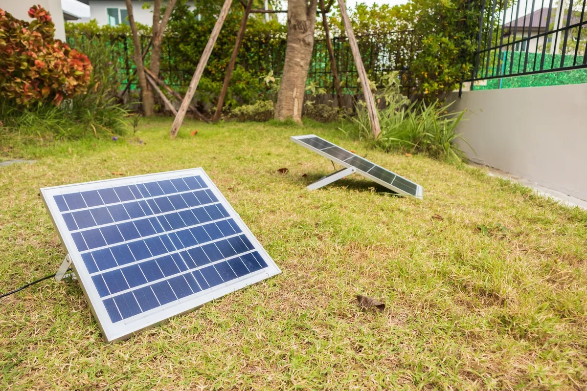
Is solar panels easy to make?
DIY panels are feasible but extremely difficult. Manual efficiency is only about 10%, far below the commercial level of 22%.
The core challenge lies in the fact that silicon wafers are extremely brittle and require vacuum lamination; otherwise, short circuits occur easily.
It is recommended to prioritize purchasing certified finished products to ensure electrical safety and a stable power supply for more than 10 years.
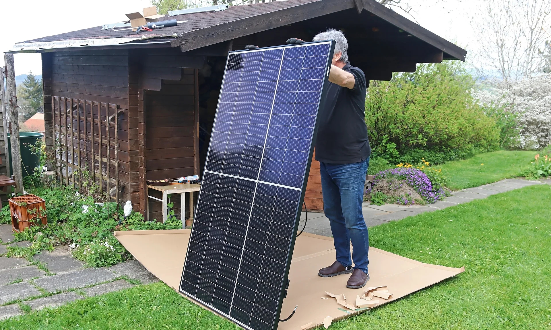
DIY Assembly
Preparation Work
Before assembly, set up a flat workbench with an area of no less than 2 square meters, covered with a 3 mm thick anti-static rubber mat to prevent micro-cracks in the silicon wafers under pressure.
The ambient temperature must be maintained between 20°C and 25°C, with relative humidity below 50%, because for every 10% increase in humidity, the oxidation rate of the tinned solder ribbon on the cell surface will increase by about 1.5 times.
Prepare a constant temperature soldering iron with a rated power of 60W to 90W, with its tip temperature error controlled within ±5°C.
Choose a digital multimeter with a precision of 0.01 V for measurement tools.
For a 100W panel, prepare 36 monocrystalline silicon solar cells of 156.75 mm × 156.75 mm, each with a nominal power of about 2.8 W, leaving 4 pieces as spare parts for operational loss, with a total budget between 36 and 40 pieces.
Cell Classification
Do not start welding as soon as you pick up the cells; perform current matching tests first. Under a simulated light source of 1,000 W/㎡, use a multimeter to measure the short-circuit current (Isc) of each cell.
The Isc of Monocrystalline Grade A cells is usually between 8.5 A and 9.1 A.
Group cells with a current deviation controlled within ±0.1A.
If an 8.0A cell is mixed into a string of 9.0A cells, the output current of the entire panel will be forced to be limited to 8.0A, resulting in a 11% power loss.
The open-circuit voltage (Voc) of each cell should be between 0.61V and 0.63V.
Through this parameter screening, the Fill Factor (FF) of the module can be increased from 70% to over 75%.
Hands-on Soldering
Soldering is divided into two steps: interconnection and busbar connection. Use tinned flat copper ribbons with a width of 1.6 mm and a thickness of 0.15 mm as interconnecting strips.
The soldering temperature is set between 360°C and 380°C.
Align the interconnecting strip with the silver main grid line on the front of the cell; the contact time between the iron tip and the silicon wafer is strictly forbidden to exceed 2.5 seconds to prevent thermal cracking of the 180 µm thick silicon wafer.
· Front Soldering: The length of the interconnecting strip should be 2 times the width of the cell plus a 5mm reserve. The solder wetting angle should be less than 90 degrees, ensuring a pull force greater than 1.2 N/mm.
· Back Series Connection: Solder the lead-out wire of the first cell's interconnecting strip to the back solder point of the second cell. Every 12 cells are connected in series, completing three strings in total.
· Spacing Control: The physical spacing between cells should be maintained at 2 mm to 3 mm, with space reserved to handle the thermal expansion of materials in outdoor temperatures of 70°C.
After soldering is completed, use a multimeter to measure the voltage of each string; the open-circuit voltage of 12 cells in series should stabilize within the range of 7.2V to 7.5V.
Layering and Laying
The bottom layer is 3.2mm thick low-iron ultra-white patterned tempered glass, with a light transmittance greater than 91%.
Lay a layer of 0.45 mm thick EVA (Ethylene-Vinyl Acetate) film on the glass.
Evenly place the 3 soldered cell strings on the EVA. Maintain a safety creepage distance of 15 mm between the cell strings and the glass edge.
Use a busbar strip with a width of 5 mm and a thickness of 0.2 mm to connect the 3 cell strings in series.
Cover the cells with a second layer of 0.45 mm EVA, and finally lay a 0.3 mm thick TPT (Tedlar-Polyester-Tedlar) white backsheet.
The TPT backsheet provides insulation voltage resistance of over 1000 V and possesses anti-UV aging capabilities for more than 20 years.
At this point, the total thickness of the entire "sandwich" is approximately 4.4 mm.
Sealing and Pressurizing
If you do not have an industrial vacuum laminator costing more than 20,000 yuan, manual assembly should use neutral weather-resistant silicone sealant.
Apply sealant in the inner groove of the 30mm × 25mm aluminum alloy frame; the injection volume should account for 60% to 70% of the groove.
Press the glass laminate into the frame and apply a uniform pressure of about 5 kg to expel internal air bubbles.
If the bubble diameter exceeds 2 mm, condensation will occur due to temperature differences after one year of use, leading to corrosion of the cell grid lines.
Install an IP67 rated junction box on the back of the module, with 2 pieces of 10A Schottky diodes embedded inside for bypass protection.
The voltage drop of the diode should be lower than 0.4V to reduce the hot spot effect caused by partial shading.
After sealing is completed, let it sit at 25°C for 24 hours until the glue is completely cured; the peel strength after curing should reach more than 40 N/cm.
Final Electrical Performance
Tested under noon sunlight, the open-circuit voltage Voc of the 100W module should be between 21V and 22.5V, and the operating current Imp should reach above 5.5A.
Inspection Items | Standard Data | Allowed Deviation |
Output Power | 95W - 105W | ±5% |
Insulation Resistance | >100MΩ | Tested under 500V DC |
Frame Perpendicularity | 90° | ±0.5° |
Module Weight | 7 kg - 8 kg | Depending on frame thickness |
The cost per watt of DIY panels is about 2.1 yuan, while the price of commercial finished products is between 3.5 yuan and 4.5 yuan per watt.
This means that through five hours of manual labor, you can save about 140 yuan to 240 yuan on a 100W specification.
Although the annual degradation rate of manually encapsulated panels may reach 1%, slightly higher than the 0.7% of industrial parts, for DIY off-grid systems or monitoring power supply, the investment recovery cycle is usually shortened to 18 to 24 months.
Industrial Manufacturing
Silicon burned out from furnaces
Inside the crystal pulling furnace, high-purity (99.9999999%, i.e., 9N grade) electronic-grade polysilicon is heated to a melting point above 1420°C.
Using the Siemens method or Czochralski method (Cz method), seed crystals are lifted at a speed of 1 to 3 mm per minute to grow cylindrical monocrystalline silicon ingots with a diameter usually of 200 mm or 300 mm.
The silicon ingots are then processed into square slices by diamond wire cutting machines. Currently, the mainstream M10 specification size is 182mm × 182mm, while the larger M12 specification reaches 210mm × 210mm.
The loss during cutting (kerf loss) is controlled between 50µm and 60µm, and the thickness of the silicon wafer has been reduced from 200µm in the early days to the current 150µm to 160µm.
This reduction in thickness directly lowers silicon material costs by about 15%, while posing higher requirements for the precision of subsequent mechanical gripping, with the breakage rate needing to be controlled below 0.05%.
Data Point: A 12-roller cutting machine can process about 500 silicon ingots per day, and the surface roughness of a single silicon wafer must be less than 0.5 µm to ensure the uniformity of subsequent diffusion processes.
Electrifying Silicon Wafers
After entering the cell production stage, silicon wafers undergo etching, diffusion, and coating.
Current industrial mainstream PERC (Passivated Emitter and Rear Contact) or TOPCon (Tunnel Oxide Passivated Contact) technologies can increase the theoretical photoelectric conversion efficiency of cells to between 23% and 25.5%.
In a high-temperature diffusion furnace at 850°C, phosphorus atoms are injected to form a PN junction, with the depth controlled between 0.3 µm and 0.5 µm.
To reduce light reflection, a pyramid-shaped textured surface is formed on the silicon wafer surface through chemical acid cleaning, with a height of about 3µm to 5µm.
Subsequently, a 70 nm to 80 nm thick silicon nitride anti-reflection film is deposited on the surface using Plasma Enhanced Chemical Vapor Deposition (PECVD), giving the silicon wafer its common deep blue or black appearance.
Data Point: Silver paste is one of the most expensive auxiliary materials in cell production. The silver paste consumption for the front and back of each cell has been optimized from 120 mg to about 80 mg. The number of silver wires (busbars) has increased from 5 to 12 or even 16 (MBB technology), which shortens the current collection path and reduces internal resistance loss by about 2%.
Machine String Soldering
During the module assembly phase, automatic stringers connect cells together at a speed of 3,000 to 4,000 pieces per hour.
Industrial-grade solder ribbons usually consist of flat tinned copper ribbons with a thickness of only 0.18 mm.
The machine completes instantaneous heating within 0.1 seconds through infrared welding technology, ensuring solder joint strength reaches over 1.5 N/mm.
To increase the light-receiving area, factories generally adopt Half-cut technology, which involves cutting 182mm cells in half with a laser.
The physical logic behind this is: the current is halved, and the resistance loss is reduced to one-quarter of the original (P=I²R), increasing the output power of the entire module by 5W to 10W.
In addition, the gap between cells is compressed to 0.5 mm or even arranged in a shingled manner, making the module space utilization reach over 95%.
Data Point: During the soldering process, each string of cells undergoes online EL (Electroluminescence) testing. By applying a current of about 10 A to make the cells glow, high-definition cameras can capture micro-cracks or dark spots with a diameter of over 0.1 mm.
Encapsulation and Compaction
Module lamination is the step that ensures a 25-year lifespan. The workbench area of an industrial laminator usually exceeds 6 square meters, capable of processing two large modules simultaneously.
Lamination process parameters are usually set as: vacuuming for 5 minutes (pressure reduced below 100 Pa), followed by pressing for 10 to 15 minutes at a temperature of 145°C to 155°C.
During this process, the 0.5 mm thick EVA or POE film melts under heat and undergoes a cross-linking reaction, with the degree of cross-linking needing to reach over 85%.
In this state, the film tightly bonds the 3.2 mm tempered glass, cell strings, and TPT backsheet.
The water vapor transmission rate of the TPT backsheet must be lower than 0.1 g/㎡·24 h to ensure the internal circuits are not oxidized.
Data Point: The iron content of tempered glass needs to be controlled below 150 ppm to guarantee a light transmittance of over 91.5%. After lamination, the thickness precision deviation of the entire module is controlled within ±0.2 mm.
Framing and Boxing
Laminated modules need to be fitted with 6063-T5 hardness aluminum alloy frames.
The frame surface undergoes a 12 µm thick anodizing treatment to resist salt spray corrosion.
The junction box is attached to the outlet position on the back of the module using silicone.
The junction box usually integrates 3 bypass diodes with rated currents of 20A to 30A to cope with the hot spot effect that large-sized modules might generate.
Special corner protectors will be installed at the four corners of the module, and high-viscosity neutral silicone sealant will be injected.
This encapsulation method ensures that the module can withstand wind loads of 2400 Pa and snow loads of 5400 Pa without physical damage to the internal silicon wafers.
Data Point: The pace of industrial production lines is extremely fast. From glass feeding to final product packaging, the online time for a single module is about 25 to 30 minutes. Highly automated assembly lines have reduced labor costs per megawatt (MW) by more than 80%.
Factory Health Check
The final step is the Flash Test.
Under standard laboratory test conditions (STC: 1000 W/㎡ light intensity, 25°C cell temperature, AM1.5 spectrum), the simulator emits a high-precision flash with a duration of 10 to 100 milliseconds.
The tester captures voltage and current data in real-time and draws the IV curve.
The factory will "bin" the modules according to the actual power, for example, 540W, 545W, 550W at 5W intervals, with the power positive tolerance controlled between 0 and +5W.
Additionally, the module must pass high-voltage withstand tests of over 2000 V, with leakage current less than 50 µA.
Performance Indicators | Industrial Standard Data | Degradation Rate Prediction |
Module Efficiency | 21% - 23% | First Year < 1% |
Fill Factor (FF) | 78% - 82% | Annual Degradation < 0.45% |
Operating Temperature (NOCT) | 45°C ± 2°C | Power retention rate after 25 years > 85% |
Insulation Strength | > 100MΩ | IP68 Protection Level |
Current industrial manufacturing has diluted the cost of 550W grade modules to about 0.12 to 0.15 USD per watt.
This scale effect and 0.1mm level precision control are technical gaps that home DIY environments cannot bridge.
Needs
What Cells to Buy
Currently, the market mainstream is 166mm × 166mm monocrystalline silicon Grade A cells.
The open-circuit voltage (Voc) of a single cell is usually around 0.64 V, with a peak current (Imp) of about 10.5 A and a peak power (Pmax) of about 5.4 W.
To form a 12V charging system, 36 cells are usually required in series to obtain an idle voltage of about 23V and a load voltage of 18V.
For a 24V system, 72 pieces in series are needed.
Suppliers must be requested to provide flash test reports during procurement to ensure that the current deviation of the same batch is less than 0.1 A.
If Grade B cells or defectives with a current difference exceeding 5% are mixed in, the power of the entire panel will be reduced according to the performance of the worst cell, resulting in an energy loss of more than 20%.
Spec Name | Physical Dimensions (mm) | Conversion Efficiency (%) | Power per Cell (W) | Suggested Use |
M6 Monocrystalline Cell | 166 × 166 | 22.3% | 5.4W - 6.1W | RV/Rooftop DIY |
M10 Monocrystalline Cell | 182 × 182 | 22.8% | 7.2W - 7.8W | High-power Fixed Power Station |
G12 Monocrystalline Cell | 210 × 210 | 23.1% | 10.1W - 10.5W | Industrial Grade Assembly |
When handling these silicon wafers with a thickness of only 170 µm to 190 µm, vacuum suction pens or 100% nitrile gloves must be used; oils left by direct finger contact will cause grid line oxidation within 3 to 6 months.
Picky with Welding Materials
The choice of soldering materials directly affects the internal resistance of the module. You need two specifications of tinned copper ribbons: interconnecting (Tab Wire) and busbar (Busbar).
For 166 mm cells, it is recommended to use an interconnecting ribbon with a width of 1.6 mm and a thickness of 0.2 mm, with a tin content ratio usually of Sn60/Pb40 or lead-free Sn96.5/Ag3.0/Cu0.5.
The thickness of the tin layer on the ribbon surface should be between 20 µm and 40 µm to ensure wetting can be completed within 2 seconds at a soldering temperature of 370°C.
If the internal resistance of the ribbon is too high, when the current reaches 10 A, the heat power at the connection will exceed 5 W, which not only lowers the output voltage but may also generate hot spots above 80°C.
Flux must be a no-clean type with a solid content below 5%.
Strongly acidic flux is easy to solder with, but residual ions will corrode the silver paste grid lines on the silicon wafer surface within one year, scrapping the cell.
For a 200W module, the required ribbon length is about 35 meters; it is recommended to prepare an extra 15% margin for bending and jumping.
Sealing Layer Materials
To ensure that solar panels can withstand more than 20 years of wind and sun, the quality of encapsulation materials cannot be compromised.
The outermost layer must use 3.2 mm thick ultra-white patterned tempered glass.
Regular glass has a higher iron content, absorbing about 5% to 10% of near-infrared light, while the light transmittance of ultra-white glass must reach over 91.7%.
Below the glass are two layers of 0.45 mm to 0.5 mm thick EVA film.
EVA undergoes a cross-linking reaction at 140°C, forming a transparent and waterproof elastomer.
If the degree of cross-linking is lower than 75%, the film will gradually turn yellow under UV irradiation; for every 10% yellowing, power generation efficiency will drop by about 8%.
The bottom layer is a TPT or TPE backsheet, usually 0.3 mm thick.
The backsheet must not only provide insulation (voltage resistance must be greater than 1000 V DC), but also have an extremely low water vapor transmission rate (less than 1.5 g/㎡·24 h).
Material Layer | Recommended Thickness (mm) | Core Function Parameters | Lifespan Expectancy |
Ultra-white Tempered Glass | 3.2mm | Light transmittance > 91% | 30 years |
EVA Film | 0.45mm | Cross-linking Degree 80% - 90% | 25 years |
Monocrystalline Silicon Cell | 0.18mm | Efficiency 22.5% | 25 years |
TPT/KPE Backsheet | 0.3mm | Insulation Voltage 1500V | 25 years |
Frame and Box
Assembled laminates require a 6063-T5 aluminum alloy frame to provide mechanical strength.
The frame thickness is recommended to be between 30 mm and 35 mm, with the surface anodized layer thickness reaching over 12 µm to prevent acid rain corrosion.
The junction box must have an IP67 or IP68 waterproof rating.
Inside, 2 to 3 Schottky diodes (such as 15SQ045 or 20SQ045) need to be configured.
The role of these diodes is to prevent the "hot spot effect", where if part of the cells are shaded by leaves, the diode can bypass that part of the current.
The rated current of the diode should be at least 1.5 times the maximum current of the cell, usually 15A or 20A.
The matching cable should use 4 mm² dedicated PV DC cable, which has double insulation and UV resistance, capable of long-term operation even in a 90°C environment.
The contact resistance of the MC4 connector should be less than 0.5 mΩ to reduce power loss under high current.
Tools Ready
A constant temperature soldering station of about 90 W is needed, capable of precisely adjusting the temperature between 300°C and 450°C.
Regarding measurement tools, the DC current range of the digital multimeter must support continuous measurement above 10A.
If conditions allow, prepare a simple vacuum generator and silicone pad to simulate the exhaust process of an industrial laminator.
Before encapsulation, use a 500V insulation resistance tester to check the insulation value between the backsheet and the frame; the standard reading should be greater than 100MΩ.
For a standard 200W DIY project, your space and main material costs are roughly as follows:
· Work Space: At least 3 square meters of clean and dust-free area.
· Cell Cost: Calculated at 0.15 USD per watt, about 30 USD.
· Auxiliary Material Cost: Glass, frame, EVA, backsheet, and junction box total about 40 to 50 USD.
· Total Budget: About 80 to 100 USD (excluding one-time tool purchase costs).
The entire assembly cycle, from cell screening to final sealing and curing, takes about 8 to 10 working hours for a single person.