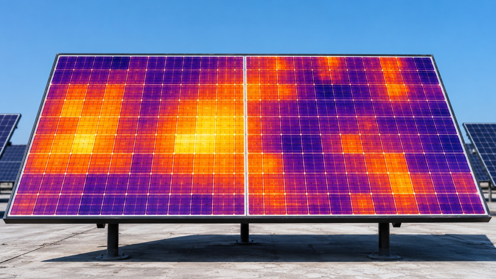
Uneven cell temperatures without visible shading usually come from electrical mismatch, hidden cracks, damaged ribbons or solder joints, local shunts, bypass-diode problems, corrosion, uneven rear-side light, or different cooling conditions. A sharply defined cell-shaped hot area is more likely to be an electrical problem. A smooth temperature band crossing several cells is more likely to come from wind, mounting, or a thermal-camera error.
"No visible shading" does not always mean every cell receives exactly the same light. A thin mineral film may be difficult to see. A torque tube may affect the rear side of a bifacial module. Reflected infrared radiation may also create a false hot area.
Thermal imaging shows where abnormal heat appears, but it generally cannot identify the exact defect on its own. The result should be checked against visible inspection, operating data, I-V measurements, and electroluminescence imaging when needed.[1]
Why Cells Heat Differently
Within one series-connected cell path or substring, the same current passes through each cell. Modern solar module designs may contain several series and parallel paths, but one weak cell can still limit the path in which it is connected.
Two main mechanisms produce abnormal heat.
Resistive heating occurs in damaged ribbons, busbars, solder joints, connectors, and other current-carrying parts:
P = I2R
Heat rises with resistance and with the square of current. If current rises from 5 A to 10 A while resistance stays unchanged, the heating term rises from 25R to 100R. The current has doubled, but resistive heating has increased four times.
This is why a weak solder joint may look normal under low sunlight but become clearly hotter around midday when module current is higher.
Reverse-bias heating occurs when a weak cell cannot produce the current required by the other cells in its series path. Its voltage may become negative, causing it to absorb power instead of producing it:
Dissipated power is approximately current × reverse voltage.
For example, a weak cell carrying 10 A at a reverse voltage of 5 V would dissipate about 50 W as heat. This is only an example, not a universal hot-spot value or replacement threshold. Actual heating depends on the cell, module circuit, bypass diode, irradiance, temperature, and inverter operating point.
The inverter also affects the thermal pattern because its maximum power point tracker changes system current and voltage as sunlight and temperature change. The same fault may be difficult to see in the morning and obvious later in the day.
Normal Temperature Differences
A module surface is rarely at one exact temperature. Normal differences can be caused by:
- Wind cooling one side more strongly
- The aluminum frame cooling the edges
- Mounting rails carrying heat away from the backsheet
- Lower airflow behind the center of a roof-mounted module
- Nearby vents, walls, parapets, or tracker parts
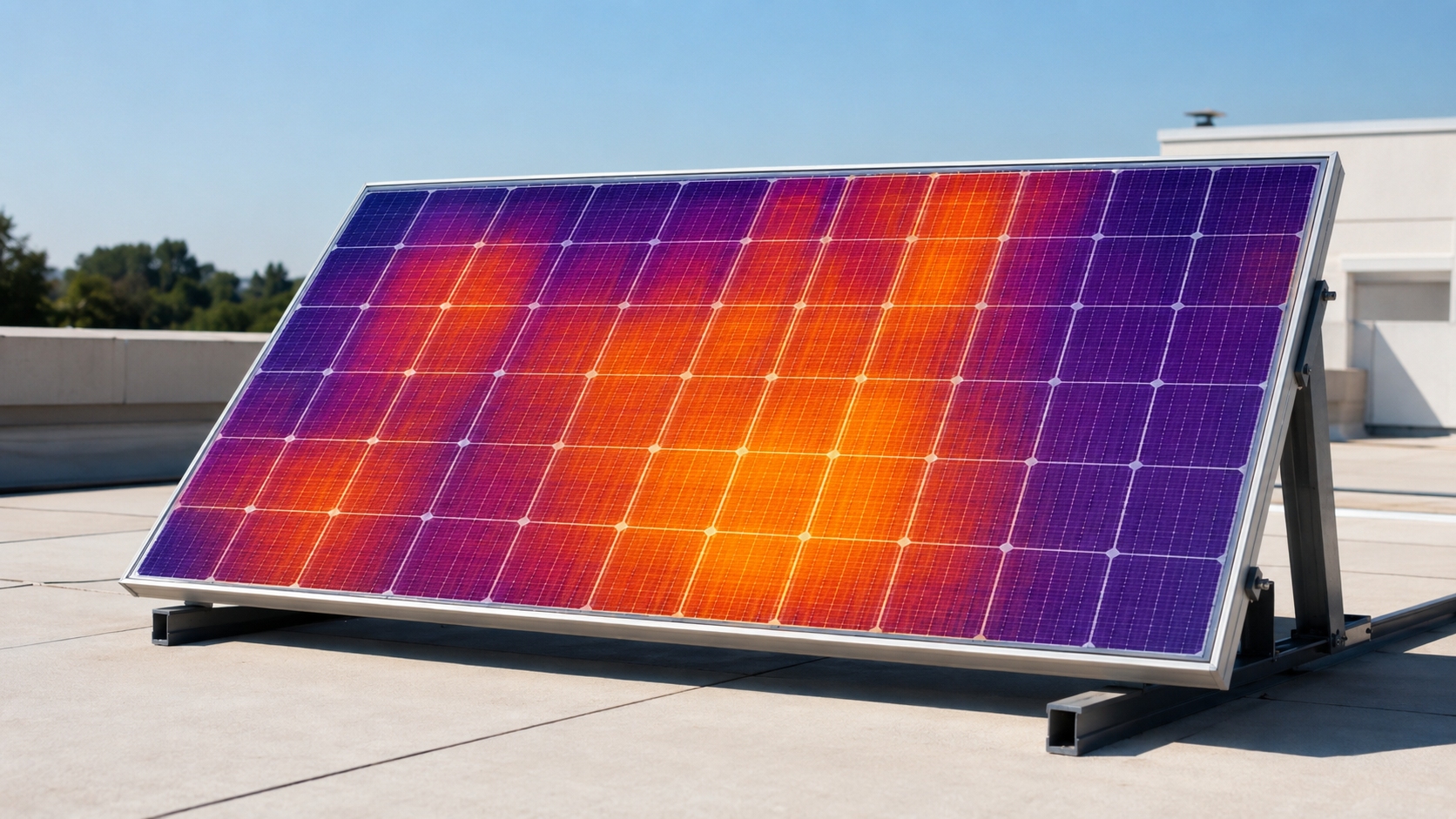
These patterns are normally smooth, cross several cell boundaries, and often appear on nearby modules in similar positions. A sharply defined hot area that matches one cell, half-cell, ribbon, or solder point is less likely to be normal cooling.
Cloud movement can also create misleading images. A typical module may need roughly 5 to 15 minutes to reach a new thermal balance after a major change in sunlight, air temperature, or wind. IEA PVPS recommends stable conditions and generally favors irradiance above about 600 W/m² for useful outdoor infrared inspection.[2]
For example, if a cloud passes at 12:00, an image taken at 12:02 may still show temporary temperature differences. Rechecking the module around 12:10 to 12:15 under stable sunlight gives a more useful comparison.
Do not judge a module only by its highest temperature. A more useful value is ΔT, the temperature difference between the suspect area and a suitable reference measured under the same conditions.
Consider these two examples:
- A cell at 62°C beside cells at 58°C has a ΔT of 4°C.
- A cell at 62°C beside cells at 42°C has a ΔT of 20°C.
The suspect cell has the same absolute temperature in both examples, but the second pattern is much more unusual. These numbers are examples, not fixed pass-or-fail limits.
A suitable reference may be:
- An adjacent healthy cell in the same module
- A nearby module of the same model
- A module with the same orientation and mounting position
- The same area recorded during an earlier inspection
The reference should have similar sunlight, current, airflow, and mounting. IEC TS 62446-3 covers outdoor infrared inspection equipment, environmental conditions, procedures, reporting, and personnel competence. It does not define one universal surface-temperature limit for every module and installation.[3]
Cell Mismatch and Reverse Bias
Cells from the same production batch are similar but not identical. Manufacturers sort cells so that cells with similar electrical characteristics are assembled together. Mismatch can also develop after installation because of cracking, moisture, corrosion, heat exposure, material variation, or electrical stress.
A mismatched cell may show:
- One full cell or half-cell running hotter
- Lower module or string current
- Reduced maximum power
- Lower fill factor
- A step in the I-V curve
- Repeated heating at the same cell position
Moderate mismatch may cause only a small temperature rise. Severe mismatch can force the weak cell into reverse bias.
Reverse-bias heat may spread across the full cell or concentrate at a crack edge, shunt, or damaged junction. Fault size alone does not show severity. A broad warm cell may be less urgent than a very small point with a high peak temperature, growing ΔT, or visible browning.
Long-term heating can damage the encapsulant, metallization, solder joints, backsheet, adhesive layers, and electrical insulation. Visible warning signs include:
- Brown or dark cell areas
- Bubbles
- Delamination
- Backsheet discoloration
- Burn marks
Bypass diodes limit reverse voltage across a group of cells, but they do not prevent every hot spot. A small local defect may heat before the diode starts conducting, and mild mismatch may not activate the diode.
Microcracks and Inactive Areas
Silicon cells are thin and brittle. They can crack during manufacturing, transport, unpacking, installation, frame twisting, wind loading, snow loading, hail impact, or repeated thermal cycling.
A crack does not automatically cause power loss or heat. If metal fingers and busbars still cross the crack, both sides may remain electrically connected.
A crack can become more serious through the following process:
- A crack forms in the silicon.
- Metal conductors continue bridging the crack.
- Mechanical movement and temperature cycles widen the damage.
- Some conductors break.
- Part of the cell becomes weakly connected or isolated.
- Current passes through fewer remaining paths.
- Local current density and resistance increase.
- Repeated heating causes further damage.
The total string current does not necessarily increase. A similar current is being forced through a smaller conductive area.
Common thermal patterns include:
- A hot triangle
- A hot corner
- One hot side of a cell
- An irregular hot section
- A warm strip near a crack boundary
Crack risk depends more on electrical isolation than on crack length. A crack that separates 10% of a cell area does not always cause exactly 10% power loss. Current may still reach that area through fingers, busbars, or multi-wire connections.
A long crack with several working current paths may therefore have less effect than a short crack that separates one corner from every collection path. IEA PVPS failure guidance assesses cell cracks according to their electrical, performance, and safety effects rather than visible length alone.[4]
Hidden cracks are normally better confirmed with EL imaging than with a front visual inspection. Tongwei's article on EL testing before module installation explains how EL can reveal cracks, soldering defects, inactive areas, and cell mismatch that are difficult to see through the glass.
Fingers, Busbars, Ribbons, and Solder Joints
The current-collection system includes thin metal fingers, larger busbars, interconnection ribbons, and solder or bonded joints. Damage at each point can produce a different thermal pattern.
Broken fingers reduce current collection within part of a cell. The break itself may not be the hottest location because little current may pass through the broken section. More useful signs include a darker EL area, uneven current collection between busbars, and heating near the remaining conductive paths.
Busbar damage affects a main current path within the cell. It may create a straight warm area, a hot point, or one side of the cell running warmer.
Ribbon faults affect the connection between cells. A partly bonded ribbon may carry current through a small contact area and create a hot line or point near the cell edge.
Weak solder joints may work at low current but become resistive when current rises. They may produce normal output in the morning, lower power later in the day, intermittent optimizer alarms, or a rounded I-V curve.
If one ribbon disconnects, the remaining paths carry a larger share of the current. Their temperature and stress rise, which can cause further connection failures.
Modern multi-busbar and multi-wire cells provide more current paths than older cells with only a few busbars. One damaged path may therefore have less immediate effect, although several damaged paths can still isolate part of a cell. Tongwei's guide to high-density cell layouts and module reliability explains why current, resistance, cell spacing, interconnection design, and thermal control must be considered together.
Local Shunts
A shunt is an unwanted low-resistance path through a cell. Some current leaks through the defective area instead of following the intended electrical path.
Possible causes include:
- Cell-edge defects
- Junction damage
- Contamination
- Moisture
- Corrosion
- Metallization defects
- Manufacturing damage
- Electrical overstress
A local shunt may create a very small but intense hot spot. Camera resolution matters because a distant image may average the hot point with a much larger cool area and report a lower peak temperature.
For example, a small point at 90°C surrounded by cell material near 50°C may appear much cooler when both areas fall within the same thermal pixel. The displayed temperature depends on the hot area's size, camera resolution, focus, distance, and image-processing method.
A suspected shunt should be checked with a close, focused thermal image, a fixed temperature scale, a second viewing angle, EL imaging, and electrical measurements. Fraunhofer ISE reports that lock-in thermography can resolve temperature differences of a few milli-Kelvin and locate local shunts, series-resistance defects, and other faults inside a module laminate.[5]
Bypass Diodes and Substrings
Bypass diodes protect groups of cells called substrings. Under normal conditions, current flows through the cells and the diode does not conduct. If a substring cannot carry the required current, the diode routes current around it.
A diode may start conducting without visible front-side shading because of:
- A cracked or mismatched cell
- A disconnected ribbon
- A weak solder joint
- A local shunt
- Corrosion
- An isolated cell area
- Uneven rear-side irradiance
A traditional module may use three diodes for three similar substrings. If one substring is bypassed, the module can lose roughly one-third of its normal operating voltage.
For example, a traditional module operating near 40 V could lose roughly 12 to 14 V when one of three similar substrings is bypassed. This is not a universal value. Half-cell, back-contact, shingled, and multi-section modules can use different circuits.
An active diode is not automatically damaged. It may be working correctly because another fault has forced it to protect the substring.
A shorted diode permanently bypasses its substring. The main signs may be missing voltage and reduced power rather than one extremely hot cell.
An open diode cannot protect the substring. It may remain unnoticed until a weak cell, crack, or temporary obstruction creates mismatch. The affected cell can then experience stronger reverse voltage and heating.
NREL failure analysis found that field-failed bypass diodes can suffer thermal damage under continuous long-term forward-bias overstress.[6]
Junction-Box Heating
A warm junction box is not automatically defective. It contains diodes and electrical connections that can produce heat during normal operation.
Abnormal heating may come from:
- A bypass diode conducting for a long period
- A damaged diode
- A loose terminal
- Poor soldering
- Corrosion
- A damaged internal conductor
- High contact resistance
The location of the heat is useful:
- Heat over one diode may indicate diode conduction or diode stress.
- Heat near a cable exit may indicate a terminal or conductor fault.
- A small, sharp hot point may indicate high contact resistance.
- A broadly warm box may contain normal diode heat or several heat sources.
Compare the suspect box with boxes of the same design under similar current, sunlight, mounting, and airflow. A 5°C difference under one set of conditions cannot be compared directly with a 15°C difference recorded on a hotter, windless day.
PID, Corrosion, and Material Damage
Potential-induced degradation, or PID, is linked to voltage stress between cells and grounded module parts. Risk depends on system voltage, polarity, humidity, temperature, glass, encapsulant, cell technology, and grounding design.
Possible signs include lower open-circuit voltage, lower fill factor, lower string power, broad dark EL patterns, or several related modules showing slightly different temperatures. PID normally affects groups of cells or modules rather than one isolated hot cell.
A slightly warmer module is not enough to diagnose PID. Check whether the pattern follows the module's position in a high-voltage string and confirm it with I-V, EL, leakage, or insulation measurements. IEC 61215-1-1 includes a test for detecting PID in crystalline-silicon modules.[7]
Corrosion can increase resistance in fingers, busbars, ribbons, solder joints, junction-box terminals, and connectors. Moisture may enter through module edges, cracked backsheets, damaged glass, poor seals, cable entries, or the junction box.
Corrosion may produce warm conductor lines, hot terminal points, edge heating, or output that changes during wet weather. One dry-day inspection may not show the full problem.
Encapsulant damage can include yellowing, browning, bubbles, delamination, loss of adhesion, and moisture entry. It can reduce light transmission, change heat flow, or allow corrosion to develop.
Not every delaminated area becomes hot. An air gap may appear warmer or cooler depending on optical absorption and heat transfer. IEA PVPS identifies encapsulation, cell cracking, PID, junction-box connections, glass, and technology-specific degradation as continuing reliability issues in modern modules.[8]
Hidden Deposits
A module may look clean from the ground while still carrying a thin deposit such as:
- Mineral residue
- Salt film
- Fine dust
- Pollen
- Dried cleaning marks
- Oil mist
- Thin bird residue
These deposits can reduce light without creating an obvious dark shadow. They can also change the glass surface's infrared behavior, creating an apparent temperature difference.
Inspect the glass from different angles. When cleaning is allowed by the manufacturer, clean the suspect area and repeat the scan under similar sunlight, wind, current, camera angle, and temperature scale. Do not compare a morning image directly with a midday image.
Soiling is estimated to cause average global PV energy losses of about 4% to 7%, but the loss at one site can be lower or much higher depending on climate, deposit type, rainfall, module angle, and cleaning practice.[9]
Bifacial Modules
A bifacial module receives light from both sides. The front may have no visible shading while the rear receives uneven light from:
- Torque tubes
- Support piles
- Cable trays
- Foundations
- Vegetation
- Snow or water
- Uneven ground color
- Nearby module rows
A repeated thermal pattern in the same structural position across several modules often points to rear-side conditions rather than identical cell failures.
The pattern may change with sun position, tracker angle, vegetation, snow, or ground moisture. Compare modules at the same tracker angle and inspect the structure behind the module.
Product construction should also be checked before interpreting the image. Tongwei's TWMNH-66QD module, for example, lists a mass-production bifaciality of 90% ± 5%. A module with high rear-side response can be more sensitive to uneven rear irradiance, but actual field gain and thermal behavior still depend on albedo, structure, row spacing, and installation conditions.
Camera Errors
A thermal camera receives both emitted and reflected infrared radiation. Reflections can come from the sky, clouds, buildings, trees, nearby equipment, or the camera operator.
Reflection is more likely when:
- The pattern moves when the camera moves
- The shape changes with viewing angle
- The pattern does not follow cell boundaries
- Similar shapes appear on several modules
- Front and rear images do not agree
Automatic color scaling can also make a small difference look severe. A red area may be only 3°C warmer than its surroundings in one image and 20°C warmer in another. Check the actual temperature and ΔT, not only the color.
Focus, distance, and camera resolution matter. A blurred image spreads a small hot point over a larger area. A long measurement distance averages hot and cool surfaces into the same pixels.
Typical reference settings may use an emissivity near 0.85 for front glass and near 0.95 for many polymer backsheets, but these are not universal values. The correct setting depends on the actual material, coating, viewing angle, reflected temperature, and camera method.
Avoid shallow viewing angles because reflection from the sky becomes stronger.
Test Conditions
A useful outdoor thermal inspection normally requires:
- Strong, stable sunlight
- Irradiance above about 600 W/m²
- Low or moderate wind
- No fast-moving clouds
- A working inverter
- Normal operating current
Higher irradiance makes many mismatch and resistance faults easier to see because the module carries more current. The array should normally be operating rather than left at open circuit.
A useful field record may look like this:
- Irradiance: 760 W/m²
- Air temperature: 31°C
- Wind speed: 1.5 m/s
- Suspect cell temperature: 67°C
- Reference cell temperature: 52°C
- ΔT: 15°C
These figures are only an example of how to record an inspection. A ΔT of 15°C is not an automatic replacement rule. The thermal pattern, operating current, power loss, visible damage, repeat behavior, and module design must also be considered.
Record the following during an actual inspection:
- Irradiance
- Air temperature
- Wind speed
- Module and string position
- Inverter status
- Maximum and reference temperatures
- ΔT
- Time and camera angle
- Camera model and resolution
- Measurement distance
- Front or rear inspection
- Emissivity and reflected-temperature settings
- Fixed or automatic temperature scale
If clouds, wind, or operating current changes during the inspection, repeat the image after conditions stabilize.
How to Read the Pattern
| Thermal pattern | Possible causes | Best next check |
|---|---|---|
| One full hot cell | Mismatch, reverse bias, distributed shunt | I-V curve and EL image |
| One hot half-cell or irregular section | Crack, isolated area, local shunt | Close thermal image and EL test |
| Hot corner | Isolated crack area, edge shunt, deposit, reflection | Change camera angle and inspect the glass |
| Thin hot line | Busbar, ribbon, solder joint, conductor resistance | Compare with the internal conductor layout |
| Whole substring different | Bypass-diode operation, shorted diode, connection fault | Check module voltage and I-V curve |
| Hot junction box | Conducting diode, damaged diode, terminal resistance | Compare equivalent junction boxes |
| Whole module slightly warmer | Disconnection, PID, shorted diode, different cooling | Confirm current, voltage, and airflow |
| Smooth temperature gradient | Wind, frame conduction, mounting, rear clearance | Compare nearby modules and airflow |
| Pattern moves with camera | Infrared reflection | Repeat from another angle |
Inspection Steps
- Check that the thermal image is focused and uses a suitable temperature scale.
- Change the camera angle to rule out reflection.
- Confirm that sunlight, wind, and operating current are stable.
- Compare the suspect cell with adjacent cells.
- Compare the module with a suitable reference module.
- Inspect the front, rear, edges, junction box, and cables.
- Review inverter, string, or optimizer data.
- Use I-V testing when power or substring behavior is unclear.
- Use EL imaging when cracks or current-collection faults are suspected.
- Decide whether to monitor, inspect soon, or isolate the fault urgently.
Visible inspection should check for glass cracks, delamination, discoloration, surface deposits, backsheet damage, burn marks, frame distortion, loose cables, junction-box damage, and connector heating.
Review Tongwei's photovoltaic module installation manual before cleaning, disconnecting, testing, or removing a module.
I-V and EL Testing
An I-V curve shows how current changes with voltage. Useful signs include:
- Reduced current from optical loss, weak cells, or mismatch
- A step caused by substring mismatch or bypass-diode operation
- A rounded knee caused by increased series resistance
- Abnormal slope near short circuit caused by shunting
- Missing voltage from a bypassed or failed substring
I-V results should be corrected for irradiance and cell temperature. One curve shape can have more than one cause, so it must be compared with thermal and visible evidence.
EL imaging applies current to the module and records weak light from electrically active cell areas. It can show microcracks, weakly connected regions, broken fingers, ribbon faults, poor solder joints, PID patterns, and uneven current collection.
A dark EL area does not always carry zero current. EL brightness also depends on test current, exposure, temperature, series resistance, shunting, camera sensitivity, and test connections.
Thermal imaging shows where heat develops during operation. EL imaging shows how electrical activity is distributed during the test. Using both methods gives a more reliable diagnosis.
When to Act
There is no single temperature limit that applies to every module and inspection condition. A difference of a few degrees may come from wind, but the same difference becomes important when it follows one cell, repeats under stable conditions, or is linked to lower power.
Monitor the module when the temperature difference is small and stable, there is no visible damage, power remains normal, and the pattern does not grow during repeat inspections.
Arrange an inspection soon when a cell-shaped pattern returns, ΔT is increasing, string data is abnormal, or a crack, ribbon, solder, or diode fault is suspected.
Take urgent professional action when there is smoke, melting, burning odor, exposed conductors, burn marks, severe connector heating, or rapidly increasing temperature.
Safety
PV modules produce DC voltage whenever they receive light.
Do not:
- Open an energized junction box
- Disconnect connectors under load
- Touch exposed conductors
- Spray cold water on hot glass
- Step on modules
- Test diodes without electrical isolation
- Remove modules without an approved shutdown procedure
A damaged module can remain energized after the inverter stops. DC arcs can continue when a poor connection is separated under load.
IEC 61730-1 defines module construction requirements intended to reduce electrical shock, fire, and mechanical hazards.[10] IEC 61730-2 defines the safety tests used to detect component failures that could cause fire, electric shock, or injury.[11]
Connector work, junction-box testing, I-V tracing, insulation testing, EL testing, and module replacement should be completed by trained personnel using suitable DC-rated equipment.