Why Perform Electroluminescence (EL) Testing Before Photovoltaic Module Installation
Hidden defects, soldering defects, and cell electrical mismatch are three major groups of latent problems that solar modules can develop during manufacturing, shipping, and installation.
Any one of these problems can reduce actual power below the nameplate rating. The size of the loss depends on the defect area, electrical isolation, module circuit design, and bypass-diode behavior; severe or combined defects can produce losses above 10%.
Defect Group | Typical Examples | What EL Shows |
Hidden Defects | Microcracks, inactive cells, hot-spot susceptibility | Dark lines, inactive regions, and abnormal luminescence patterns |
Soldering Defects | Poor solder joints, broken busbars, loose ribbon interconnects | Localized dark areas, interrupted current paths, and uneven transition bands |
Cell Mismatch | Non-uniform output, low-current cells, string power loss | Brightness differences between cells or across one cell |
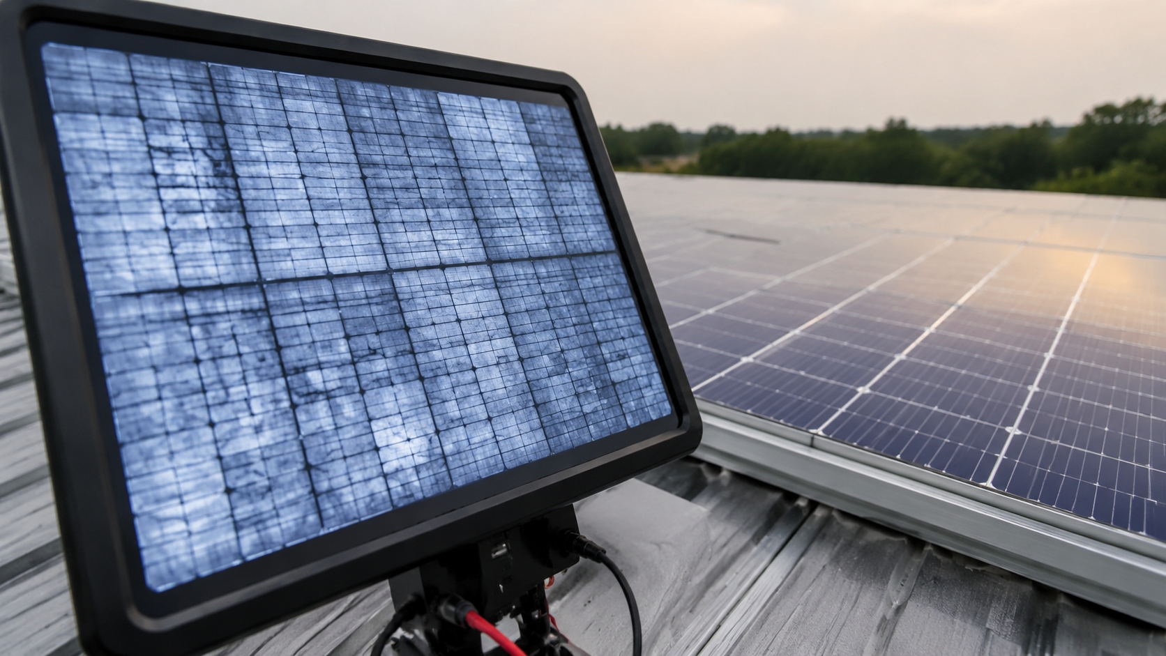
Electroluminescence testing uses the near-infrared emission produced when a crystalline-silicon solar cell is forward biased. The silicon EL signal peaks near 1150 nm and can be captured by suitable silicon CCD/CMOS cameras or by InGaAs detector systems, depending on sensitivity, wavelength response, exposure requirements, and the inspection environment.[1][2][3]
Defects often appear as dark lines, dark regions, or uneven brightness in the resulting image. Exposure time is equipment-dependent: professional systems may capture an image in under one second, while lower-sensitivity field systems may require several seconds or longer.
EL testing adds spatial evidence that a conventional I-V curve cannot provide by itself.
IEA PVPS Task 13 work on field reliability identifies manufacturing defects, transport damage, installation damage, and field-induced degradation as important contributors to module underperformance. It does not establish a universal figure showing that more than 60% of early degradation comes from defects missed before shipment.[4]
In our Tongwei cell and module production lines, modules are screened with inline EL as part of the factory quality flow, which includes inspection before shipment and checks at key production stages. This two-stage approach supports utility-scale quality control, where one weak module can reduce the performance of a series-connected string.
Hidden Defects
Microcracks
Microcracks are among the most common latent defects in crystalline-silicon cells. Their openings are often too small for unaided visual inspection, while EL imaging can reveal their orientation, length, branching pattern, and electrically inactive areas.
l EL signature:Thin dark lines, branching lines, diagonal cracks, or dark cell areas that have become electrically isolated.
l Capture time:A professional EL system may expose a module in under one second, while many field or modified-camera systems require 1 to 30 seconds or more, depending on sensitivity and ambient light.
l Field relevance:Cracks can grow during transportation, installation, thermal cycling, and mechanical loading.
l Power impact:A visible crack does not automatically mean a large immediate power loss. The impact depends mainly on the inactive cell area and the electrical resistance across the crack.
Published research does not support a single universal statement that 5 to 12% of all modules arriving at project sites contain a crack longer than half a cell edge. The observed rate varies widely with supplier, packaging, transport route, sampling plan, module design, and the defect threshold used by the inspector.
On one internally documented utility-scale project, a portable EL sample found an 8% microcrack rate. Root-cause analysis pointed to insufficient packaging cradle cushioning, and the rate dropped below 1% after thicker foam was introduced.
Internal Crack Grade | Internal Definition | Internal Disposition |
Class A | Crack crossing busbars or creating a significant electrically isolated area | Reject |
Class B | Crack not crossing busbars but longer than 20 mm | Engineering review |
Class C | Crack shorter than 20 mm without a significant inactive area | Review under the internal acceptance plan |
Our EL imaging reaches 0.5 mm per pixel. The Class A, B, and C grading above is an internal quality-control scheme; IEC 61215 does not define this crack-classification system or prescribe a universal EL pass/fail limit. IEC 61215-1 covers module design qualification and type approval rather than a factory EL defect grading system.[5]
Our field data show that cracks crossing current-collection paths create more risk than short cracks that remain electrically connected. Cracks perpendicular to busbars can produce power loss above 10% when they isolate a large part of a cell, but crack direction alone does not determine the loss.
In our experience, finding microcracks at the loading dock costs far less than replacing modules after they have been mounted on a tracker. The exact cost ratio depends on labor, access equipment, transport, lost generation, and warranty recovery, so a universal two-hundred-times figure should not be applied to every project.
In portable EL inspections for installer partners, a common pattern is a diagonal crack from one corner toward another. This can be linked to handling stress during cell, module, framing, transport, or installation operations, and the root cause should not be assigned to one handling step without supporting process evidence.
Flash testing may show little immediate loss when a cracked cell remains electrically connected. EL can reveal the crack before thermal and mechanical cycling causes the separated area to become inactive.
A crack visible in EL is not automatically power-relevant, but it can become power-relevant as the electrical connection deteriorates.
For third-party acceptance surveys, the sample size should be based on lot size, project risk, supplier history, transport conditions, and the contractual acceptance plan. A 5% sample can be a practical starting point for some lots, but it is not a universal standard.
Inspectors should compare images taken at two forward-current levels rather than referring to "dark and bright bias polarity." IEC EL imaging is based on forward bias, and low-current imaging can help distinguish cracks that are more likely to be power-relevant. A single-current scan can miss or misinterpret some defects, but no universal factor-of-two undercount applies to every inspection.[2][3]
Dead Cells
Cells or cell regions that appear fully dark in an EL image are electrically inactive under the applied test condition. A dark cell does not always prove that it produces no photocurrent; the same appearance can result from an open interconnection, severe shunting, an inactive junction, or a measurement-current path problem.
l Possible upstream causes:Material contamination, non-uniform diffusion, severe junction defects, laser-process damage, broken metallization, or disconnected interconnects.
l Electrical effect:The affected cell can limit its series-connected substring or force the bypass diode to conduct.
l Power effect:Loss may be several percent for one affected cell, but it depends on the module layout, substring size, defect severity, irradiance, and bypass-diode state.
At a 100 MW plant producing about 1,500 to 1,800 kWh per kW each year, a 1% affected-module rate combined with a 3% to 5% loss in those modules would equal roughly 45 to 90 MWh of annual generation loss.
At common utility PPA prices, that amount normally represents hundreds to several thousand dollars per year, not seven figures of annual revenue. The lifetime value can become much larger after labor, access, replacement, downtime, escalation, and warranty recovery are included.
In our bench comparisons, modules flagged by EL for fully inactive cells delivered 4.2% less power than nameplate on average. That result is outside a typical positive-only or narrow manufacturing tolerance, although the correct comparison should use the product datasheet and measured uncertainty for the specific module.
On the Tongwei cell line, inline EL flags suspect units and routes them for review or rework before they move farther through production.
I-V testing measures the module's aggregate electrical performance; EL shows where the local electrical problem is located.
A dead or disconnected cell does not necessarily "hide" from a valid I-V test. The I-V curve may show reduced current, reduced fill factor, a step, or bypass-diode activation, but it cannot localize the failed cell as clearly as EL.
A current-limiting cell can enter reverse bias and create local heating. Repeated heating can accelerate encapsulant discoloration, delamination, interconnection damage, and backsheet aging, but a universal three-times yellowing rate is not supported across all module materials and operating conditions.[6]
For this reason, we treat a fully dark cell in the post-lamination EL scan as a hard reject rather than a downgrade candidate. We do not release modules with a confirmed inactive cell into a B-grade bin for residential, commercial, or utility applications.
Catching inactive cells with EL also reduces warranty exposure related to local heating and material degradation in modules that may otherwise show only an aggregate electrical anomaly during flash testing.
Hot-Spot Risk
Hot-spotting is one of the most serious performance and safety risks in an operating PV module.
When a cell is shaded, cracked, mismatched, or internally defective, it can enter reverse bias and dissipate power from neighboring cells as heat. Under severe test conditions, local cell temperatures can exceed 150 degrees Celsius.[6]
Temperature Point | Technical Meaning |
40 to 50 degrees Celsius | Typical NOCT/NMOT-type range for many modules under standardized assumptions, with the exact value depending on module design, mounting, irradiance, wind, and ambient temperature[7] |
50 to 70 degrees Celsius | Field operating range that can occur under warm or high-irradiance conditions; IEA PVPS also discusses hot cells rising above a typical module operating range of 50 to 70 degrees Celsius under mismatch or shading stress[6] |
Above 150 degrees Celsius | Can significantly damage polymeric materials and accelerate discoloration, delamination, and embrittlement[6] |
183 degrees Celsius | Melting point of Sn63Pb37 eutectic solder[8] |
About 217 to 220 degrees Celsius | Typical melting range of common SAC305 lead-free solder[9] |
A local temperature above 150 degrees Celsius can damage the encapsulant and backsheet, but it is not automatically high enough to melt common solder. Solder failure becomes more likely as the joint approaches the alloy's melting range, while prolonged exposure below that range can still accelerate fatigue and material damage.
l EL screening:Abnormal dark regions and unusual luminescence patterns can identify cells that need further investigation.
l Confirmation:Controlled reverse-bias characterization and infrared thermography can be used as complementary methods.
l Timing:A three-second scan is possible on some automated systems, but test time is equipment- and method-dependent.
IEA PVPS identifies cell cracking, shading, reverse bias, and local heating as linked risks. It does not provide a universal statistic showing that every EL-flagged module has a 5.3-times higher first-year thermal-event rate.[6]
On one commercial and industrial rooftop project, EL pre-screening covered 3,500 modules and identified 42 units for hot-spot review, a 1.2% flag rate. Infrared thermography confirmed abnormal heating in the flagged units, and they were replaced before commissioning.
This result should be described as confirmation of the flagged set, not as 100% diagnostic accuracy unless the unflagged population was also tested and false negatives were evaluated.
Specifying EL pre-screening in the acceptance protocol, together with module reliability records, can lower operating risk and strengthen the asset owner's commissioning evidence.
A single thermal event can cost several times the module's purchase price after access equipment, labor, lost generation, investigation, replacement, and inverter restart are included. The multiplier varies by project and should not be fixed at five to ten times for every site.
We have seen hot-spot incidents develop from cells that appeared borderline during production and became thermally unstable within the first months of operation. Our internal threshold therefore uses additional factory screening beyond the IEC 61215-2 hot-spot endurance test, which is a design-qualification test procedure rather than a universal factory EL pass/fail rule.[10]
IEC 61215 does not provide a single reverse-bias voltage limit that can be used as a universal internal screening threshold. IEC 61215-2 defines design-qualification test procedures, including hot-spot endurance testing.
For existing fleets, portable EL combined with handheld or drone-based infrared thermography is a practical option. The lowest-cost method depends on plant size, access, nighttime work, electrical isolation, and inspection scope, and all records should be archived with commissioning and warranty documentation.[3]
Soldering Defects
Poor Solder Joints
The electrical continuity of a module depends heavily on solder quality. Poor solder joints can appear as localized dark areas where the cell tab meets the interconnect ribbon.
Insufficient solder coverage, poor wetting, contamination, excessive intermetallic growth, or a cold joint can increase contact resistance and reduce local EL intensity.
l Defect frequency:Solder-process defects are an important manufacturing category, but a universal 15% to 20% share of all defects is not supported across every factory and technology.
l Sn63Pb37 alloy:The melting point is 183 degrees Celsius.[8]
l Common SAC305 lead-free alloy:The melting range is about 217 to 220 degrees Celsius.[9]
l Process peak:A soldering process commonly operates above the alloy melting range, subject to ribbon coating, flux, heating method, dwell time, cell technology, and equipment qualification.
Lead-free SAC solder normally requires a higher process temperature than eutectic tin-lead solder. A process window should therefore be tied to the actual alloy, flux system, ribbon coating, equipment, dwell time, and product qualification.
Across the specific batches included in our internal joint-quality audits, we found a Pearson correlation of 0.82 between EL grayscale variation and joint shear strength. This makes EL useful as a non-contact screening proxy for the audited process window, but it does not replace destructive ribbon-pull or shear testing when mechanical joint strength must be verified.
On one export shipment, inline EL flagged about 3% of modules with a batch-level soldering anomaly. The investigation traced the problem to a heating-system temperature sensor that read about 15 degrees Celsius low.
After the sensor was replaced and the process was requalified, the defect rate fell below 0.1%, and the backlog was reworked within 72 hours.
Pairing EL screening with Tongwei's published process documentation closes the loop between detection and corrective action.
When EL grayscale variation suggests a soldering problem, our next step is cross-sectional analysis together with a ribbon-pull test on samples from the same production batch. This helps separate a cell-ribbon interface problem from a deeper metallization or paste-related problem.
We have used this workflow to identify silver-paste supplier changes that could have passed standard incoming inspection.
EL-based screening can also reveal a module-level current-path abnormality caused by ribbon, busbar, connector, or junction-box connection problems. Flash testing can quantify the resulting power loss, while EL helps locate the affected region.
For portable EL, installers should compare images at two forward-current levels and look for asymmetric or localized dark patterns. Routine reverse-bias imaging should not be presented as the default EL method because IEC TS 60904-13 defines EL imaging under forward bias.[2]
Broken Busbars
The busbar is a primary current-collection conductor on a conventional solar cell. It is commonly formed by printing and firing a conductive paste, and it carries current from the cell metallization to the interconnect ribbons.
A broken or poorly connected busbar can create a partially or fully dark cell region because current no longer reaches that area evenly under forward bias.
l Physical defect:The actual fracture gap may be only a few to tens of micrometers wide.
l EL detection:EL does not need to optically resolve the micrometer-wide gap itself; it detects the larger electrically inactive or dim region created by the interrupted current path.
l Resolution:Fine-resolution EL improves localization. IEA PVPS practice groups include image resolutions of 0.2 mm per pixel or better, 2.0 mm per pixel or better, and 5.0 mm per pixel or better for different inspection purposes.[3]
Common causes include metallization defects, paste or firing-profile problems, thermal-expansion stress, printing non-uniformity, soldering stress, and mechanical loading during production or handling.
The power effect of one broken busbar depends on the number of busbars or wires, the break location, parallel current paths, cell technology, and the size of the isolated region. The loss can be small or substantial; a universal 20% to 40% loss for every single broken busbar is too broad.
Multiple severe busbar or interconnection failures can produce an obvious flash-test failure.
During one supplier audit, we sampled 500 cells from each of three vendors. One supplier showed a 4.6% busbar-break rate, substantially above our internal acceptance window, and about 150,000 suspect cells were held from production.
The 0.5% to 1.2% comparison should be treated as an internal or dataset-specific benchmark, not a universal industry norm.
Tongwei cell production uses combined AOI and EL inspection. Internal validation has shown detection sensitivity above 98.5% for the defined defect set and validation protocol, although sensitivity always depends on defect labeling, image quality, threshold selection, and validation design.
Cross-sectional microscopy on the failed audit samples showed fractures near silver-crystallite grain boundaries rather than at the silver-silicon interface. The evidence pointed to a firing profile about 30 degrees Celsius too hot for the paste formulation used at that time.
After the vendor changed paste and added post-fire inspection, the next audit showed a 0.7% break rate, inside our acceptance window.
Where microscopy is not available, infrared imaging under controlled electrical loading can provide a secondary indicator because a resistive or partially conductive busbar may heat locally. The test conditions must be controlled so that the thermal pattern is not confused with shading, contact resistance elsewhere, or ambient non-uniformity.[3]
Loose Ribbon Interconnects
Loose or detached ribbon interconnects can appear in EL images as irregular bright-to-dark transition bands between cells. This pattern differs from a single poor solder joint because the problem can affect a larger ribbon-to-busbar contact area and create uneven current distribution.
l Possible causes:Poor solder wetting, insufficient ribbon coating, contamination, incorrect heating profile, encapsulant cure problems, and excessive module flexing.
l Field incidence:Ribbon and interconnection failures are recurring field defects. Some datasets may report an 8% to 12% share among selected failure populations, but that range is not a universal site-failure rate.
l Wafer size:Larger cells and longer interconnections can change thermo-mechanical stress, but reliability also depends on half-cell layout, wire count, ribbon geometry, encapsulant, glass structure, and mounting.
In our 200-cycle thermal-cycling test from minus 40 to plus 85 degrees Celsius, modules flagged for loose ribbons showed an average 28% increase in ribbon resistance, compared with less than 3% for clean modules.
This is correctly described as thermal cycling rather than thermal shock. The result is an internal screening dataset and should not be treated as a universal resistance threshold for every module design.
EL inspection is non-contact and maps the module's current distribution without opening the junction box. It pairs well with thermography and electrical testing for field troubleshooting.
Tongwei's internal certification framework classifies confirmed ribbon looseness as Class A under its internal ribbon-defect disposition rule. This is an internal quality grade; IEC 61215 does not provide a Class A ribbon-looseness category.[5]
On three rooftop projects, installers performed EL after modules were placed and provisionally secured but before final clamp torque. This sequence helped identify marginal contacts before final mechanical loading changed the symptom.
During this sequence, modules must remain safely supported and fastened throughout inspection.
Adding this inspection step may require about half a day on some projects, depending on array size, string isolation, darkness, crew size, and equipment. It has prevented commissioning rework on several supported projects.
Tongwei's installation guidance recommends additional EL checks on larger or higher-risk projects, including projects above 1 MW where contract requirements call for them. Our field-service team uses portable EL equipment to support site checks.

Cell Mismatch
Non-Uniform Cell Output
Even after cell binning, cells inside one module can show output variation under operating conditions. In EL images, non-uniformity may appear as a brightness gradient across a cell or as irregular bright and dark regions that change with applied current.
l Diffusion:Non-uniform emitter sheet resistance can change current collection and recombination.
l Metallization:Finger-width, height, continuity, and contact-resistance variation can create uneven brightness.
l Firing or sintering:Temperature gradients can produce non-uniform contact formation.
The 90 to 110 ohms-per-square sheet-resistance band, the plus-or-minus 10% limit, the 12 to 18 micrometer finger-height target, and the plus-or-minus 3 micrometer variation are process-specific internal targets. They are not universal limits for PERC, TOPCon, HJT, back-contact, and other cell technologies.
Our internal quantitative EL threshold flags a cell when its grayscale root-mean-square deviation exceeds 15% under the defined camera, current, exposure, and cell-technology conditions. We selected this value after two years of comparison with flash-test and process data.
Internal correlation work for the evaluated process window showed a coefficient of 0.78 between the EL uniformity score and module fill factor. This makes the score useful for screening and binning, but the relationship should be recalibrated for each cell technology, camera system, current level, and production line.
In field and factory reviews, EL has identified non-uniform cells before deployment, and module power returned to specification after the affected cell or module was reworked.
Each module leaving our Tongwei reliability-cleared line carries an AI-scored EL uniformity result, and sub-spec units are routed according to the internal disposition plan.
For bifacial modules, rear irradiance can increase operating current and therefore change the absolute energy penalty caused by a front-side current bottleneck. The effect depends on rear irradiance uniformity, bifaciality, circuit layout, and operating conditions.[6]
Our internal dataset showed a rear-side mismatch penalty 1.5 to 2 times the front-side penalty for the same grayscale deviation under the tested conditions. That multiplier is not universal and should not be applied without matching the rear-irradiance and circuit conditions.
Developers sourcing bifacial modules can request quantitative EL uniformity data together with flash-test records, while recognizing that AI scores are supplier-specific unless the scoring method and acceptance threshold are disclosed.
Low-Current Cells
Low-current cells usually glow less than neighboring cells under the same forward-bias condition while retaining some luminescence. This helps distinguish them from cells or regions that are fully inactive under the test condition.
industrial and commercial module solutions
l Diffusion non-uniformity:Can alter emitter sheet resistance, carrier collection, and recombination.
l Broken fingers:Reduce current collection from part of the cell.
l Lifetime non-uniformity:Raises recombination and reduces effective cell current.
l Shunting:Low shunt resistance is a separate leakage mechanism and should not be described simply as the direct result of low phosphorus concentration.
A single cell with short-circuit current 5% to 10% below its series neighbors can reduce module power by several percent. A 2% to 6% module-level loss is plausible for some layouts, but the actual value depends on substring design, bypass-diode behavior, irradiance, and the number of affected cells.
Our EL screening threshold is 70% of the string-average luminescence intensity. Any module below that threshold is re-imaged before it is flagged, because intensity also depends on camera response, temperature, current, exposure, and cell technology.
On one ground-mount project, EL pre-screening of about 2,000 modules identified 187 modules with low-current cells, a 9.35% flag rate. Across the affected modules that were reworked, average peak power increased from 535 W to 548 W, an uplift of about 2.4%.
The 13 W increase across 187 affected modules equals about 2.43 kW of recovered DC nameplate capacity. At an annual specific yield of 1,500 to 1,800 kWh per kW, this corresponds to roughly 0.09 to 0.11 GWh over 25 years before degradation, availability, clipping, and other losses are applied.
Data presented at Tongwei industry events supports the same practical conclusion: correcting low-current cells before installation is usually cheaper than removing, transporting, reworking, reinstalling, and recommissioning modules after the plant is operating.
EL can also show localized dim regions in modules returned from logistics. However, partial shade during unpowered storage does not itself create current degradation.
Uneven mechanical pressure, moisture exposure, temperature, contamination, and handling damage during storage can create or reveal localized defects. In our returns from three logistics providers, localized EL abnormalities were found in 0.5% to 1.2% of returned modules, often near lower pallet rows.
Adding a protective tarp can help control moisture, contamination, and weather exposure, but the benefit should not be described as "blocking shade." Storage duration, pallet support, stacking load, water protection, and handling procedures are the relevant controls.
Keeping outdoor storage as short as practical and improving pallet protection reduced the observed signature to near zero in later shipments. EL provided a quantitative check without opening the laminate.
String Power Loss
String power loss is a direct consequence of current mismatch.
In a traditional 60-cell or 72-cell full-cell module, cells are arranged in series-connected substrings protected by bypass diodes. Modern half-cell modules often add parallel branches, so it is not accurate to state that every cell in every current module design is connected in one uninterrupted series chain.
Tongwei engineering deep-dives
l Current limitation:Within a series path, current is limited by the lowest-current element.
l Bypass action:A bypass diode conducts when the affected substring develops enough reverse voltage to forward-bias the diode; it does not wait for one cell to become "fully reverse-biased" under a single universal threshold.
l EL value:EL identifies the cell or region with lower luminescence and maps the aggregate electrical loss to a physical location.
EL scan time may be similar to flash-test time on a high-throughput automated line, but this is not universal. Field EL can take longer because of electrical isolation, darkness, camera positioning, exposure, and image processing.
IEC 60904-1 defines procedures for measuring photovoltaic I-V characteristics. The I-V curve quantifies current, voltage, fill factor, and maximum power, while EL provides spatial diagnostic evidence.[11]
A cell with current about 10% below its series neighbors can reduce module power by roughly 2.5% to 4% in some designs. Two or three affected cells can push the loss into the high single digits or above 10%, but the result depends on circuit architecture and bypass activation.
The strategic value of EL is that it can reveal the physical source of mismatch before modules are permanently racked and connected, rather than after the plant is producing below expectation.
On one large project, EL analysis identified underperforming cells, and replacement restored module power to the design range while avoiding a prolonged underperformance claim.
Tongwei's high-precision cell and module binning keeps current spread within a narrow internal window. A plus-or-minus 1% equivalent tolerance is reasonable only when tied to the stated current level, bin width, measurement uncertainty, and product specification.
Full-coverage EL and current binning provide two different controls: EL screens spatial defects, while binning reduces mismatch between otherwise acceptable modules.
When modules come from multiple production batches, EPC teams should compare flash-test current data and EL records before assigning modules to strings. Mixing batches with different current-bin centers can increase mismatch even when each module passes its own specification.
On internal projects, racks mixing production batches showed 2% to 3% power differences compared with batch-consistent racks. This is a project-specific result, not a guaranteed loss for every mixed-batch installation.
For multi-batch deliveries, an EL- and flash-data compatibility matrix can reduce avoidable string mismatch. Batch mixing is one possible source of underperformance, but it should not be described as the single most common source for every greenfield plant.
Taken together, EL testing is a central pre-installation inspection tool for the grouped latent-defect categories discussed above: microcracks, inactive cells, hot-spot susceptibility, soldering and interconnection defects, busbar breakage, and cell or string mismatch.
EL reduces diagnostic uncertainty, but it does not create a single universal failure-rate reduction or return-on-investment figure for every PV project.
IEA PVPS Task 13 supports the use of EL and infrared imaging for identifying module defects and assessing risk. It does not establish a universal reduction in first-year failure rate from 3.2% to below 0.5%, and it does not establish a universal inspection return above 20 times.[3]
The business case depends on module value, defect prevalence, sampling or full-inspection cost, labor, site access, replacement cost, energy price, warranty recovery, and the probability that a detected defect would become power- or safety-relevant.
Tongwei integrates EL inspection into its module quality flow and pairs it with cell and module binning. These controls support multi-decade performance, but IEC 61215 qualification and factory EL inspection do not by themselves guarantee a specific 25-plus-year service life for every module in every environment. IEC 61215-1 states that test results are not construed as a quantitative prediction of module lifetime.[5]