Why Photovoltaic Cells Are Critical for Energy Conversion Efficiency
Photovoltaic cells are critical because they directly convert sunlight into electricity with 15-22% efficiency (up to 47% in labs), using semiconductor materials like silicon to generate clean energy without moving parts, reducing losses and enabling scalable renewable power solutions.
How Light Becomes Electricity
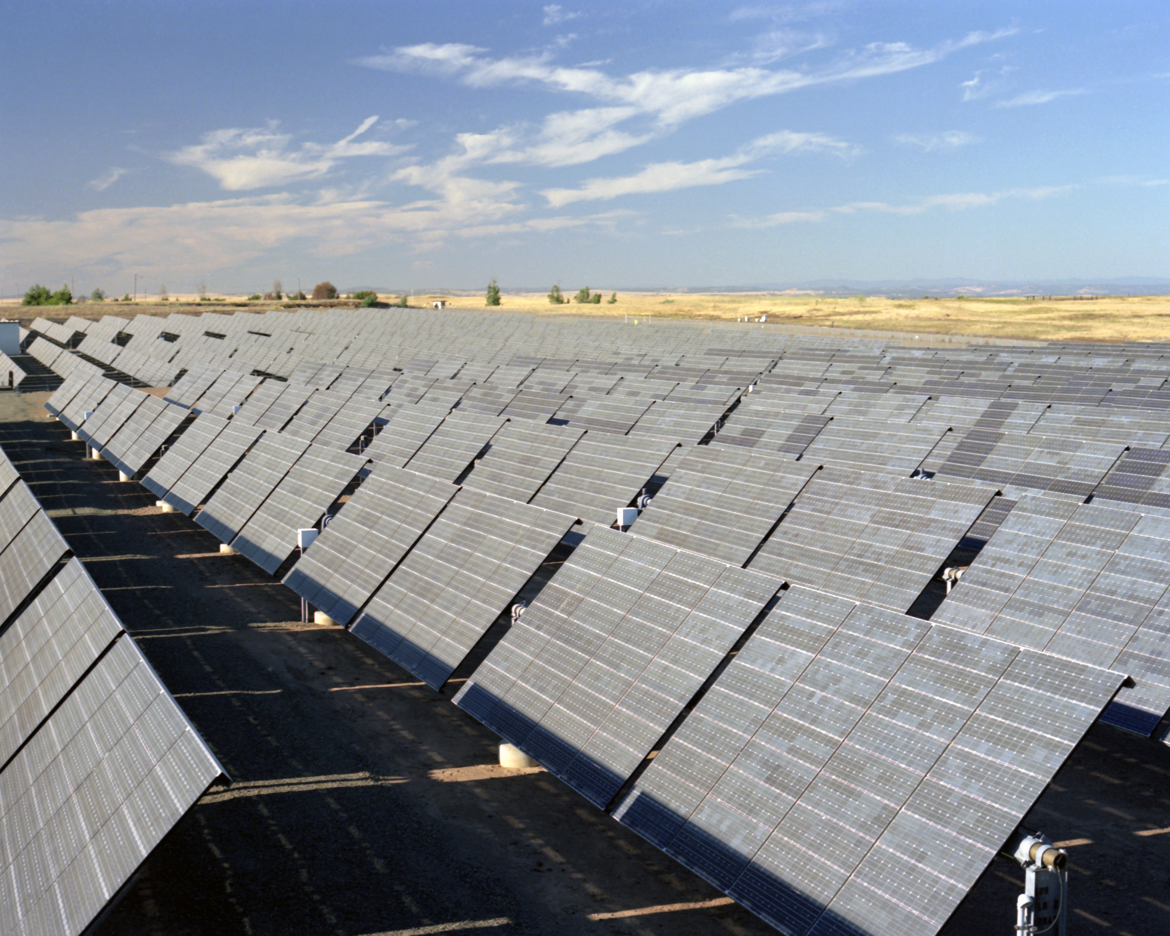
When sunlight hits a solar panel, about 15-22% of the energy is converted into usable electricity—depending on the cell technology. A typical 1.6 m² silicon panel under full sun (1,000 W/m²) generates 300-400 watts, enough to power a laptop for 6-8 hours. The process relies on the photovoltaic effect, where photons with energy ≥1.1 eV (silicon’s bandgap) knock electrons loose in the semiconductor material. Monocrystalline cells achieve 22-24% efficiency in labs, but real-world conditions (dust, heat, shading) drop this to 18-20%.
Photon Absorption:
· Sunlight delivers ~1,000 W/m² at sea level, but only photons with wavelengths <1,100 nm (near-infrared and visible light) can be absorbed by silicon.
· ~30% of solar energy is lost immediately because photons either have too low energy (<1.1 eV) or too much (excess heat).
Electron Excitation:
· Each absorbed photon generates 1 electron-hole pair in the silicon lattice.
· In PERC cells (Passivated Emitter Rear Cell), a rear aluminum oxide layer reflects unused photons back, boosting efficiency by 1-2% absolute.
Current Flow:
· The electric field in the p-n junction separates electrons and holes, creating 0.5-0.6 volts per cell.
· A standard 72-cell panel stacks these to produce 36-40 volts DC under load.
Energy Losses:
· 5-10% loss occurs from resistive heating in cell interconnects (typically 100-200 µm thick silver busbars).
· 3% loss happens due to reflection (anti-reflective coatings reduce this to 1%).
00001.
Critical Data Points:
· Best commercial panels (TOPCon, HJT) reach 22-23% efficiency, but cost 0.30−0.40/W versus 0.20−0.25/W for standard PERC.
· Thin-film technologies (CIGS, CdTe) max out at 15-18% efficiency but perform better in low-light and high-heat environments.
Why This Matters:
A 10% increase in conversion efficiency directly cuts system costs by 0.10−0.15/W, reducing payback time from 8 to 6 years for residential installations. Innovations like tandem cells (stacking silicon with perovskite) aim for 30%+ efficiency by 2030, potentially halving the required rooftop space.
Key Parts of a Solar Cell
A solar cell is more than just a slab of silicon—it’s a precision-engineered system where each layer and module directly impacts efficiency, cost, and durability. A standard monocrystalline PERC cell contains 8-10 functional layers, from the anti-reflective coating (ARC) at the top to the back-surface field (BSF) at the bottom. The front silver busbars (typically 100-150 µm wide) collect current but block 5-8% of incoming light, while the aluminum backsheet reflects unused photons to boost efficiency by 1-2%. Modern M10 wafer-based cells (182mm × 182mm) deliver 21-23% efficiency, but their performance hinges on how well these parts work together.
Core Modules and Their Roles
Module | Material/Thickness | Function | Impact on Performance |
Anti-Reflective Coating (ARC) | Silicon nitride (70-80 nm) | Reduces light reflection from 30% to <2% | Adds 1-1.5% absolute efficiency by letting more photons reach the silicon layer. |
Emitter Layer | Phosphorus-doped silicon (0.3-0.5 µm) | Creates the p-n junction for electron flow | Thinner emitters (<0.5 µm) reduce recombination losses, improving efficiency by 0.5-1%. |
Base Layer | Boron-doped silicon (200 µm) | Absorbs photons and generates electron-hole pairs | Higher purity silicon (>99.9999%) cuts electron losses, raising efficiency 0.3-0.7%. |
Front Contacts | Silver paste (10-20 µm thick) | Collects electrons from the emitter | 5-8% shading loss from busbars; multi-wire designs cut this to 3-4%. |
Back-Surface Field (BSF) | Aluminum paste (10-30 µm) | Reflects unused photons and reduces electron recombination | PERC cells use a dielectric passivation layer to boost efficiency by 1-2%. |
Backsheet | Polymer (3-5 layers, 300-400 µm total) | Protects against moisture and UV degradation | Poor backsheets lose 0.5-1% efficiency/year due to delamination in humid climates. |
Critical Interactions Between Layers
The p-n junction (formed by the emitter and base layers) generates 0.5-0.7 volts per cell, but resistive losses in the silver busbars can waste 5-10% of power at peak current. To combat this, HJT (Heterojunction) cells replace silver with copper-plated electrodes, cutting costs by 0.05/W while maintaining 240.08-$0.12/W more than PERC.
Why Thickness Matters
· Wafer thickness: Dropping from 180 µm to 130 µm saves 0.02−0.03/W in silicon costs but increases breakage rates by 15-20% during handling.
· ARC thickness: A 75 nm silicon nitride layer optimizes light absorption for 600-1100 nm wavelengths, where silicon is most responsive. Deviating by ±10 nm cuts efficiency by 0.3-0.5%.
Durability Trade-Offs
· Standard EVA encapsulant degrades at 0.3-0.5% efficiency/year under UV exposure, while POE encapsulant slows this to 0.2%/year but costs 20% more.
· Backsheet failures cause 30% of field failures after 10-12 years, with repair costs averaging 0.15−0.20/W for rooftop systems.
Why Silicon Works Best
Silicon dominates 95% of the global solar market for good reason: it hits the sweet spot between efficiency (15-24%), cost (0.20−0.40/W), and stability (25+ year lifespan). While alternatives like cadmium telluride (CdTe) or perovskites promise lower costs or higher lab efficiencies, silicon’s 1.1 eV bandgap perfectly matches the solar spectrum—absorbing ~77% of usable sunlight wavelengths (300-1100 nm). Monocrystalline silicon cells now achieve 22-24% efficiency in production, with TOPCon and HJT designs pushing toward 25%, while costing 30-50% less per watt than thin-film alternatives at utility scale.
Silicon vs. Competing Materials
Parameter | Monocrystalline Silicon | Cadmium Telluride (CdTe) | Perovskite (Lab) | CIGS |
Efficiency (2024) | 22-24% (TOPCon/HJT) | 18-20% (First Solar) | 25-26% (small area) | 19-21% (commercial) |
Cost per Watt | 0.22−0.30 (utility) | 0.25−0.35 | $0.50+ (unstable) | 0.30−0.40 |
Lifespan | 30+ years (0.5%/year decay) | 20-25 years (1%/year decay) | <5 years (unproven) | 25 years |
Temperature Coefficient | -0.3%/°C | -0.2%/°C | -0.4%/°C | -0.3%/°C |
Scalability | 100+ GW/year production | 10 GW/year (limited Cd supply) | Lab-scale only | 3-5 GW/year |
Why Bandgap Matters
Silicon’s 1.1 eV bandgap is the Goldilocks zone for solar conversion:
· Lower bandgap materials (e.g., germanium at 0.67 eV) waste energy as heat, losing >50% of photons to thermalization.
· Higher bandgap materials (e.g., gallium arsenide at 1.4 eV) miss 30% of red/infrared light, capping real-world efficiency.
Silicon captures ~45% of the sun’s energy in the visible spectrum (400-700 nm) and 32% in near-infrared (700-1100 nm), with only 23% lost to heat.
Manufacturing Advantages
1. Supply Chain Maturity:
o Polysilicon costs have dropped 90% since 2008 to 8−12/kg, feeding 200 GW/year of wafer production.
o Diamond wire saws cut wafer thickness to 150-180 µm while reducing silicon waste to <3% (vs. 30% in 2000).
2. Durability:
o Silicon modules lose 0.3-0.5% efficiency/year, versus 1%+ for perovskites in accelerated testing.
o UV-resistant EVA encapsulants prevent >95% of moisture ingress for 25+ years in field deployments.
The Cost-Efficiency Tradeoff
· PERCsilicon cells deliver 21-22% efficiency at 0.22/W, while HJTcells hit 240.28/W.
· CdTe panels are 5-10% cheaper in desert climates (thanks to their -0.2%/°C temperature coefficient) but suffer 2-3% lower efficiency in cloudy regions.
Measuring Energy Conversion Rates
Solar panel efficiency ratings don't tell the full story. While lab tests show monocrystalline silicon hitting 24-26% under ideal conditions, real-world systems typically operate at 15-18% system-level efficiency due to losses from wiring, inverters, and environmental factors. The gap between STC (Standard Test Conditions) and actual performance can reach 10-15%, costing a 5kW residential system 200−300/year in lost energy production. Precise measurement matters because every 1% efficiency drop equals 0.03−0.05/W in lifetime revenue loss for utility-scale projects.
"Field measurements vary by ±5% just from using different pyranometers. Calibrated Class A sensors reduce this to ±2%, but add 1,500−3,000 per monitoring station."
The core metric—energy conversion efficiency—is calculated by dividing DC power output (in watts) by irradiance (W/m²) × panel area (m²). But real-world complications arise:
· Spectral mismatch: Silicon responds best to 600-900 nm light, but standard pyranometers measure 300-2,800 nm. This creates 3-5% overestimation of usable energy in cloudy climates.
· Angle of incidence loss: At 45° sun angle, panels lose 4-8% of potential yield even with anti-reflective coatings.
· Soiling effects: 0.2-0.5% daily efficiency loss occurs from dust accumulation; in deserts, unwashed panels lose 15-25% monthly output.
Since silicon loses 0.3-0.5% efficiency per °C above 25°C, accurate measurements require:
1. Back-of-module sensors (error: ±1.5°C) instead of ambient air readings (error: ±5°C)
2. NOCT (Nominal Operating Cell Temperature) adjustments, typically 45-48°C for rooftop arrays, which reduce STC ratings by 12-15%
Inverter & Wiring Losses
· String inverters waste 3-5% of energy through conversion inefficiencies, while microinverters cut this to 1-2% but cost 0.10−0.15/W more.
· DC wiring loses 1.5-3% over 100 feet of 10-gauge cable; undersized wiring can double these losses.
Real-World Performance Factors
Solar panels rarely perform at their lab-rated efficiency in actual installations. While a monocrystalline panel may claim 22% efficiency under Standard Test Conditions (STC), real-world systems typically deliver 15-18% system-level efficiency due to environmental and operational factors. A 10kW residential array that should produce 40-45 kWh/day might only yield 32-38 kWh/day after accounting for temperature effects (5-12% loss), soiling (3-8% loss), and wiring/inverter losses (4-7%). These compounding factors can reduce a solar project's annual ROI by 1-2 percentage points, turning a 6-year payback into 7-8 years.
Factor | Typical Impact | Worst-Case Scenario | Mitigation Strategies | Cost to Address |
High Temperature | -0.3%/°C above 25°C (5-12% loss) | 15-20% loss in desert climates | Active cooling (+$0.10/W) or bifacial panels | 0.05−0.15/W |
Dust/Soiling | 0.2-0.5% efficiency loss per week | 25-30% loss after sandstorms | Automated cleaning (0.002−0.005/kWh) | 500−1,500/year for robots |
Shading | 15-40% output drop for partial shade | 80% loss with tree cover | Optimizers (0.15−0.20/W) | +800−1,200 per system |
Angle & Orientation | 5-10% loss from non-ideal tilt | 20% loss on flat roofs at high lat. | Adjustable racks (+0.08−0.12/W) | +800−1,500 for tracking |
Inverter Efficiency | 4-8% conversion loss | 12% loss with old string inverters | Microinverters (+0.10−0.15/W) | +1,000−2,000 per system |
Solar cells lose 0.35-0.5% of their peak power output for every 1°C above 25°C. In rooftop installations, modules routinely reach 50-60°C, causing 8-15% power loss compared to STC ratings. Bifacial panels can reduce this by 2-3% through rear-side ventilation, while water-cooled systems (used in hybrid PV/thermal setups) regain 5-7% efficiency but add 0.20−0.30/W to installation costs.
Dust accumulation follows a non-linear curve:
· Light dust (0.1mm layer): 3-5% efficiency drop
· Moderate dust (0.3mm): 8-12% loss
· Cemented dust (after rain): 15-18% loss
In California's Central Valley, unwashed panels lose 0.5% efficiency daily during dry seasons, requiring quarterly cleanings to maintain >95% of rated output.
A 10% shaded area on a string inverter system can cause 30-40% total output loss due to the "Christmas light effect" where the weakest panel drags down the entire string. Module-level power electronics (MLPE) like optimizers reduce this to 5-10% loss but increase system costs by 0.15−0.25/W.
Future Efficiency Improvements
The solar industry is pushing beyond the 25% efficiency ceiling for silicon cells, with next-generation technologies poised to redefine what's possible. While today's best TOPCon and HJT cells achieve 23-24% efficiency in mass production, tandem solar cells combining silicon with perovskites have already demonstrated 32.5% efficiency in lab settings. The National Renewable Energy Laboratory (NREL) projects 35% efficient commercial modules by 2030, which could reduce levelized solar costs by 18-22%. For a typical 5MW utility installation, this translates to 400,000−600,000 in annual savings at current electricity prices.
The most promising developments focus on spectrum-splitting architectures and defect engineering. Perovskite-silicon tandems leverage silicon's 1.1 eV bandgap for infrared light absorption while using perovskites' 1.6-1.8 eV bandgap to capture high-energy photons. Early production trials show 27-29% efficiency at 0.40−0.50/W, with potential to reach $0.30/W by 2027 through improved deposition techniques. Meanwhile, quantum dot solar cells are achieving 16-18% efficiency in research environments, offering 30-50% higher light absorption in the 300-500 nm range compared to conventional silicon.
Silicon carbide (SiC) passivation layers are reducing surface recombination losses by 45-50% in experimental cells, potentially adding 1.5-2% absolute efficiency. At the atomic scale, hydrogenation treatments are neutralizing defects in Czochralski silicon wafers, improving minority carrier lifetimes by 30-40%. For thin-film technologies, kesterite (CZTS) absorbers are now reaching 12-14% efficiency with 50-60% lower material costs than CIGS, though stability remains a challenge with 5-7% annual degradation rates in uncontrolled environments.
The shift from screen-printed silver contacts to copper electroplating is cutting front-side shading losses from 6% to 2% while reducing material costs by 60-70%. Applied Materials' Epic toolset enables <20nm precision in perovskite layer deposition, minimizing pinhole defects that previously caused 15-20% efficiency drops in early prototypes. On the wafer side, kerfless wire techniques are producing 120-130µm thin wafers with <1% breakage rates, saving 0.03−0.05/W in silicon material costs.
Every 1% increase in module efficiency reduces balance-of-system costs by 0.04−0.07/W through smaller land use and fewer mounting structures. For residential systems, 30% efficient tandem modules could enable 4.5kW systems to match the output of today's 6kW arrays, shrinking payback periods from 7 to 5 years in sunbelt states. Utilities are monitoring TOPCon-PERC hybrid lines that promise 25% efficiency at $0.23/W by 2025, which would undercut current thin-film prices while delivering 3-5% more annual yield.