5 Steps For Monocrystalline Silicon Solar Cell Production
Monocrystalline silicon solar cell production involves growing high-purity silicon ingots via Czochralski method (99.999% purity), slicing into 180-200μm wafers, texturing with NaOH/KOH solution (reducing reflectivity to <10%), doping via phosphorus diffusion (900°C, 30min), screen-printing Ag/Al electrodes (120μm line width), and laminating with EVA/glass at 150°C for 20min, achieving 22-24% efficiency.
Silicon Ingot Growth
Monocrystalline silicon ingots are the foundation of high-efficiency solar cells, with purity levels exceeding 99.9999% (6N) to minimize defects. The Czochralski (CZ) method dominates production, accounting for 85% of global monocrystalline silicon supply, due to its balance of cost (~$15-20/kg) and quality. A typical ingot weighs 300-450 kg, measures 8-12 inches (200-300 mm) in diameter, and takes 40-60 hours to grow in a 1,500°C furnace. The process consumes 50-80 kWh/kg of electricity, making energy costs a 30-40% factor in total expenses. Growth speed is critical—too fast (>1.5 mm/min) introduces defects, while too slow (<0.8 mm/min) raises costs.
The seed crystal, a small monocrystalline rod, is dipped into molten silicon and slowly pulled upward at 0.5-1.2 mm/min while rotating at 10-20 RPM. This ensures uniform crystal structure. Cooling rates must stay below 3°C/min to prevent stress fractures. Impurities like oxygen (<10 ppma) and carbon (<2 ppma) are tightly controlled—higher levels reduce cell efficiency by 0.5-1.5% absolute. Modern furnaces use magnetic field stabilization to reduce oxygen contamination by 20-30%, boosting ingot yield to 85-90% (vs. 70-75% in older systems).
Key cost drivers include:
Factor | Impact | Typical Value |
Silicon feedstock | 50-60% of total cost | $12-18/kg (2024 prices) |
Energy consumption | 30-40% of cost | 50-80 kWh/kg |
Furnace lifespan | Limits depreciation | 5-7 years (1,500-2,000 cycles) |
Labor & maintenance | 10-15% of cost | $3-5/kg |
Post-growth, ingots are trimmed to remove 5-10% of uneven ends, then tested for resistivity (0.5-3 Ω·cm) and minority carrier lifetime (>100 μs). Poor resistivity uniformity (>10% deviation) can slash cell efficiency by 1-2%. Top-tier ingots achieve 23-24% cell efficiency, while lower-grade material drops to 20-21%.
Yield optimization focuses on:
· Reducing oxygen (target: <5 ppma) via argon gas flushing.
· Controlling solidification rate (ideal: 1-1.2 mm/min) to minimize dislocations.
· Recycling 90-95% of silicon scraps (saving $5-8/kg).
The industry is shifting to larger ingots (210 mm diameter) to cut wafer costs by 15-20%, but this requires furnace upgrades (500,000−1M per unit). Breakage rates rise to 3-5% for 210 mm vs. 1-2% for 156 mm ingots, demanding better handling protocols. Total production cost for a premium 450 kg ingot is ~7,000−9,000,with wafering adding 0.08-0.12/W.
Wafer Slicing Process
Turning silicon ingots into solar wafers is a high-precision, high-waste operation where up to 40% of the silicon is lost as kerf (sawdust). The industry standard is diamond wire sawing, which cuts 200-300 μm thick wafers from 8-12 inch ingots at speeds of 1,000-1,500 m/min. Each 156 mm x 156 mm wafer weighs 6-8 grams, and a single 450 kg ingot yields 50,000-60,000 wafers. The slicing process alone accounts for 20-25% of total solar cell production costs, with wire costs ($0.02-0.05 per meter) and slurry consumption (3-5 liters per kg of silicon) being major expenses.
Key parameters affecting wafer quality:
Factor | Impact | Typical Value |
Wire diameter | Thinner = less waste | 70-100 μm (0.07-0.10 mm) |
Cutting speed | Faster = higher throughput | 1.2-1.8 m/s |
Wafer thickness | Thinner = lower material cost | 160-180 μm (target for 2025) |
Kerf loss | Wasted silicon | 120-150 μm per cut |
Breakage rate | Yield killer | 1-3% (higher for thinner wafers) |
Modern multi-wire saws use diamond-coated steel wires (lasting 3,000-5,000 cuts) to slice 2,000-4,000 wafers per hour. The wire tension must stay within 18-25 N to prevent breakage, while coolant temperature is kept at 20-25°C to avoid thermal warping. Slurry recycling can recover 60-70% of silicon kerf, saving $10-15 per kg in material costs.
Wafer thickness has dropped 30% in 10 years (from 250 μm to 170 μm), reducing silicon use by 1.5 grams per watt. However, sub-160 μm wafers face 5-8% higher breakage rates, requiring tougher handling systems (200,000−500,000 per production line). Surface roughness post-cutting is 0.2-0.5 μm Ra—too high (>1 μm) hurts cell efficiency by 0.3-0.8% due to poor light absorption.
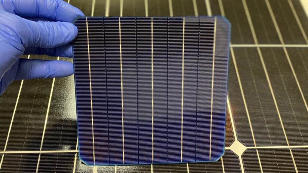
Cell Surface Treatment
After wafer slicing, the silicon surface is too smooth (0.2-0.5 μm roughness) and damaged (10-20 μm deep cracks) from sawing, which cuts solar cell efficiency by 1-2% if untreated. The industry uses alkaline texturing (KOH/NaOH solutions at 70-80°C) to create pyramid structures (3-6 μm tall) that boost light absorption by 15-20%. This process takes 8-12 minutes per batch, consumes 2-4 liters of chemicals per wafer, and adds $0.03-0.05 to cell costs. Isopropyl alcohol (IPA) is added at 5-10% concentration to speed up etching and reduce chemical usage by 20-30%.
Acid polishing (HF/HNO₃ mixes) follows texturing to remove 5-8 μm of damaged silicon, smoothing the pyramids' edges. This step is twice as fast (4-6 minutes) as alkaline etching but costs 40-50% more (0.04−0.07 per wafer) due to expensive acid handling. Over-etching(>10μm removal) risks breaking 0.5−1% of wafers (150,000 per unit) to keep surface roughness at 1-3 μm Ra—the sweet spot for low reflectance (<10%).
Post-texturing cleaning uses RCA-1 (ammonia/hydrogen peroxide) at 75-85°C to strip metal contaminants (<1 ppb target). A single 15-minute bath removes 90-95% of impurities, but 2-3% of wafers need rework due to staining or residue. DI water rinsing (10-15 liters per wafer) then flushes chemicals off, with water purity kept at 18 MΩ·cm to prevent recontamination. Drying takes 2-3 minutes in nitrogen-blown chambers, where too-fast gas flow (>20 m/s) can crack 0.2-0.5% of fragile 160 μm wafers.
Advanced treatments are gaining ground:
· Black silicon (nanotexturing) via plasma etching slashes reflectance to 2-5% (vs. 8-12% for pyramids) but adds 0.08−0.12 per wafer in equipment costs(2M per line).
· Laser doping replaces POCl₃ diffusion for selective emitters, pushing efficiency up by 0.5-0.8% but requiring 50% more energy (30-40 kWh per batch).
· Inline metrology with spectroscopic ellipsometry ($250,000 per tool) cuts process variation by 30%, raising average cell efficiency from 22.5% to 23.1% in mass production.
Cost breakdown: Texturing (0.05−0.08), cleaning (0.02-0.04), and drying (0.01−0.02) combine for 8−12% of wafer costs, plus 0.005-0.01 per wafer to neutralize 500-800 liters of acidic/alkaline effluent per hour. Top-tier lines achieve 99% yield, but typical factories lose 2-4% of wafers to etch pits, cracks, or contamination. The entire surface prep sequence lasts 25-40 minutes, with new dry processes aiming to halve that time—if they can solve current 5-7% breakage rates.
Electrical Contact Printing
Creating conductive pathways on solar cells requires ultra-precise silver paste deposition, where finger lines just 20-40 μm wide must carry 5-8 amps of current with <0.5% resistive losses. The industry standard is screen printing, which applies 80-120 mg of silver paste per cell at speeds of 1,200-2,000 wafers per hour. This process alone consumes 10-15% of total cell production costs, with silver paste (600−800/kg) being the big gest expense. Finer lines(<30μm) can boost effici ency by 0.3−0.55,000-10,000 each) that last only 20,000-30,000 prints before replacement.
Key parameters in contact printing:
Factor | Impact | Typical Value |
Finger width | Narrower = less shading | 25-35 μm (best labs: 18-22 μm) |
Paste viscosity | Affects line definition | 25-35 kcps (kilocentipoise) |
Printing pressure | Too high breaks wafers | 50-80 N (newton force) |
Snap-off distance | Gap between screen/wafer | 1.2-1.8 mm |
Curing temperature | Sintering quality | 200-250°C for 10-20 min |
Advanced pastes now contain glass frits (5-8% by weight) to improve adhesion strength (>10 MPa) and organic solvents (12-15%) for smoother flow. Double printing—where busbars are printed first (50-60 μm thick), then fingers (20-30 μm)—cuts silver use by 15-20% but slows throughput by 30%. Breakage rates hover at 0.3-0.7% for 160 μm wafers, mainly from screen contact marks or paste smearing.
Emerging alternatives:
· Electroplating: Replaces 90% of silver with copper, slashing material costs by 80% (0.02vs.0.10 per cell), but adds 3-5 process steps.
· Laser transfer printing: Achieves 15 μm lines with zero contact pressure, but machines cost $1.2-1.8M each.
· Conductive adhesives: Enable 5-10 μm contacts, but conductivity lags by 20-30% vs. sintered silver.
Cost breakdown per cell:
· Silver paste: $0.08-0.12 (60-70% of printing cost)
· Screen wear: $0.01-0.02 (5-10%)
· Energy & labor: $0.02-0.03 (15-20%)
· Defect rework: $0.005-0.01 (3-5%)
Yield killers include paste bleeding (0.5-1.2% of cells), misalignment (>50 μm error in 0.3-0.8% of prints), and cracks from high snap-off forces. Top producers achieve 98.5% printing yield, but average lines lose 2-3% to rejects. The next-gen goal is 18 μm fingers at 3,000 wph, though today’s tech still struggles with <1% breakage at 25 μm.
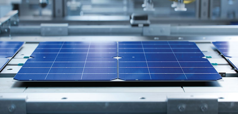
Module Assembly Steps
Turning finished solar cells into weatherproof modules is a high-speed, precision process where 60-72 cells are interconnected to create a 350-450W panel in 15-25 minutes. The glass-EVA-backsheet sandwich construction must survive 25+ years outdoors while maintaining >80% of initial power output, with module efficiency typically 1-2% lower than cell efficiency due to optical and resistive losses. Automated lines can produce one panel every 30-45 seconds, but manual labor still accounts for 20-30% of total costs in lower-tech factories.
The stringing process connects 10-12 cells in series using copper ribbons (1.5-2.0 mm wide) coated with 62/36/2 Sn/Pb/Ag solder. Each 156mm cell requires 4-6 grams of solder, adding $0.10-0.15 per panel in material costs. Hot air soldering at 250-300°C takes 3-5 seconds per joint, but temperature variations >10°C can cause 0.2-0.5% of connections to fail initial testing. Cell spacing is critical—2-3mm gaps allow for thermal expansion but wider gaps (>5mm) waste 3-5% of module area.
Lamination bonds the layers under 140-160°C heat and 15-20 kPa vacuum pressure for 12-18 minutes. The ethylene-vinyl acetate (EVA) encapsulant flows at 0.5-1.0 mm/min to fill gaps, with 400-500g used per m². Poor lamination (voids >1% area) cuts UV resistance by 30-50% and increases degradation rates to 1.5%/year versus 0.5-0.8% for quality modules. Frame assembly adds aluminum rails (1.2-2.0 kg per panel) with corner tension maintained at 40-60 N—loose frames (<30 N) allow 0.3-0.7mm/year of glass slippage.
Junction box installation handles 15-20A current with IP67-rated seals that must withstand 85°C/85% humidity testing for 1,000 hours. The bypass diodes (3-5 per panel) activate at 15-20V reverse bias, preventing hot spots that cause 0.1-0.3% annual power loss. Final testing under 1,000 W/m² simulated sunlight checks for >98% of rated power output, with 5-8% of modules needing rework for microcracks or electrical faults.
Emerging techniques include:
· Conductive adhesives replacing solder for 0.5% efficiency gain but doubling process time
· Frameless designs saving 1.2-1.8 kg per panel yet requiring 2-3x stiffer glass
· Robotic quality inspection cutting defect escape rates from 3% to 0.5%
Cost drivers break down as: glass (12−18/panel), cells(35-55), labor (8−12) ,and materials/frames(15-22). Top factories achieve 99% yield, but industry average loses 2-4% to delamination or electrical failures. The entire assembly consumes 80-120 kWh per panel, with newer lines targeting 50 kWh through laser soldering and reduced EVA cure times.