Higher reverse leakage after damp heat usually comes from one of four places: a moisture-dependent surface path, ionic contamination under electrical bias, permanent damage around passivation or the junction edge, or false leakage from the PCB/test fixture.
In practice, the first job is not to open the device. Check whether the test temperature matches, whether the fixture itself is leaking, how the reverse I-V curve changed, and whether the current comes back down after controlled drying. Strong recovery points toward a moisture-dependent path. If leakage stays high and breakdown voltage also falls, permanent damage becomes much more likely.
Verify the Test Condition First
Two samples can both be described as having “failed damp heat,” while the actual stress conditions are very different. That makes the test record the first thing to check.
| Record | Why It Matters |
|---|---|
| Temperature | Leakage itself can rise strongly with temperature. |
| Relative humidity | Controls moisture available to surfaces and materials. |
| Test duration | Separates an early shift from progressive degradation. |
| Applied voltage | Higher voltage can activate field-sensitive leakage. |
| Polarity | Ion movement and PID can depend on electric-field direction. |
| Bias during exposure | Biased and unbiased humidity can produce different failure mechanisms. |
| Measurement delay | The sample can cool and dry after leaving the chamber. |
IEC 60068-2-67 covers an accelerated steady-state damp heat test mainly for small, non-hermetically sealed electrotechnical components. It also states that the method is not intended to evaluate external effects such as corrosion or deformation.[1]
PV modules follow a different route. IEC 61215-2 defines environmental test procedures for terrestrial PV modules rather than simply applying the component test above.[2]
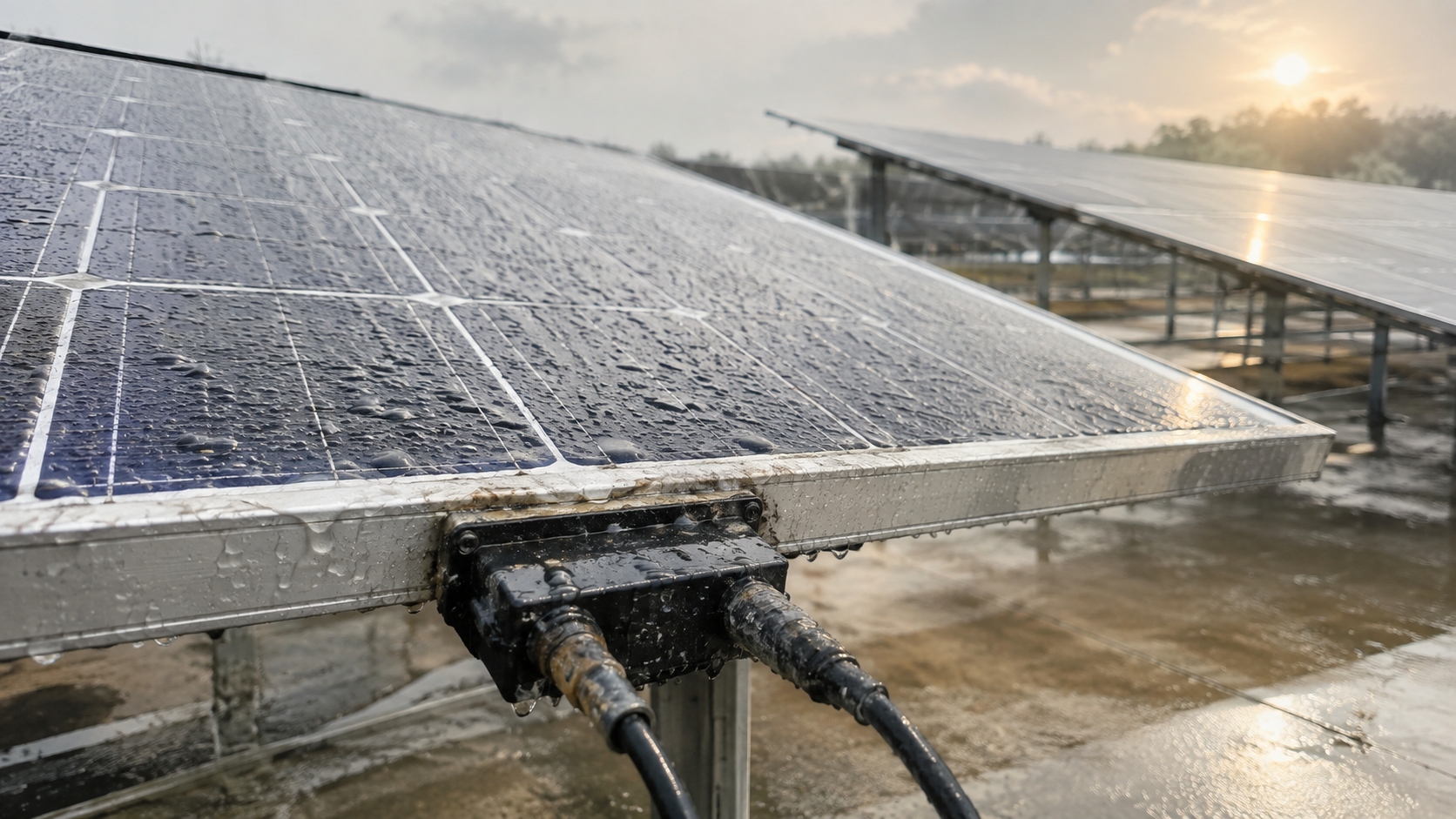
A common PV damp-heat condition is 85°C/85% RH for 1,000 hours, but that does not make it the universal definition of humidity testing. Tongwei also reports extended 3,000-hour damp heat testing for modules intended for hot and humid environments. The useful number is the one tied to the actual qualification or internal reliability requirement.
Rule Out False Leakage Before Opening the Device
Low-current measurements are easy to fool. A wet socket, dirty board, or damp cable can add enough current to make a healthy device look worse than it is.
Take the following case:
| Current Source | Initial Measurement | Later Measurement |
|---|---|---|
| Actual device leakage | 20 nA | 20 nA |
| Fixture leakage | 5 nA | 40 nA |
| Meter reading | 25 nA | 60 nA |
The meter shows a 140% increase, even though the device has not changed.
Very-low-leakage parts are even more sensitive to this problem. If the device contributes 2 nA and the fixture contributes 8 nA, 80% of the measured 10 nA comes from the fixture.
Before destructive analysis, work through the simple checks:
- measure the open fixture;
- repeat the test with a known-good reference device;
- clean and dry the socket and probe area;
- check cables and insulation;
- repeat the test on a second system if available;
- if the device is mounted on a PCB, test it separately where practical.
On a PCB, flux residue, moisture under packages, small creepage distances, wet connectors, and contaminated coatings can all create a leakage path. The meter only sees current. It does not know whether that current came from the semiconductor or from something around it.
Match the Measurement Temperature
A post-test sample that is still hot should not be compared directly with a room-temperature baseline.
If the original leakage was measured at 25°C, use the same defined temperature for the post-stress comparison unless the test procedure requires something else. Otherwise, part of the “increase” may simply be temperature.
Keep the rest of the measurement conditions aligned as well:
- reverse voltage;
- voltage ramp rate;
- measurement delay;
- instrument range;
- current limit;
- time allowed for electrical stabilization.
The time after chamber removal matters too. A device tested immediately after an 85°C humidity run can give a different result from the same device after it has cooled and lost some absorbed moisture.
Calculate Whether a Surface Path Can Explain the Current
A humidity-related path does not have to look like a short circuit. At high voltage, even hundreds of megaohms can add measurable current.
| Unwanted Resistance | 100 V | 600 V | 1,200 V |
|---|---|---|---|
| 10 GΩ | 0.01 µA | 0.06 µA | 0.12 µA |
| 1 GΩ | 0.10 µA | 0.60 µA | 1.20 µA |
| 100 MΩ | 1.00 µA | 6.00 µA | 12.00 µA |
At 600 V, reducing an unwanted surface path from 1 GΩ to 100 MΩ increases its current from 0.6 µA to 6 µA. That can happen without internal junction breakdown.
The path may sit on the die passivation, package surface, mold-compound interface, PCB, or the glass and encapsulant of a PV module.
IEC 61189-5-502 specifically uses surface insulation resistance testing to quantify harmful decreases in electrical resistance caused by materials and assembly processes.[3]
The table is only an Ohm's-law example. A real wet or contaminated surface can change resistance with voltage, humidity, temperature, and time.
Check for Ionic Contamination
If the leakage appears only when the surface is wet, soluble residue deserves attention.
Typical sources include:
- chloride;
- sodium;
- potassium;
- flux residue;
- cleaning chemicals;
- plating residue;
- process water contamination.
IEC 61189-5-504 defines process ionic contamination testing for measuring soluble ionic residues on circuit boards, components, and assemblies.[4]
A lab result showing sodium or chlorine is not enough on its own. The finding becomes useful only when it matches the failure site and the electrical behavior.
- the residue is physically close to the leakage site;
- affected devices correlate with a process or material lot;
- clean controls do not show the same shift;
- cleaning or drying reduces the current;
- the electrical behavior matches the location of the residue.
Use Bias Dependence to Find Ion-Driven Damage
One of the most useful comparisons is simple: do unbiased humidity samples stay stable while biased samples get worse?
If they do, electric field is likely part of the problem. Bias can move mobile ions and change the electrical condition of surfaces and interfaces. IEC TS 62804-1 covers potential-induced degradation in crystalline-silicon PV modules, including mechanisms in which mobile ions affect the electric field over the silicon or interact electrically with the semiconductor.[5]
NREL testing of multicrystalline-silicon PV modules at 85°C/85% RH with positive or negative 600 V system bias found strong construction-dependent leakage and degradation. In that study, chamber leakage currents reached about 100 times the levels discussed for deployed modules, and negative bias produced severe degradation in some module constructions.[6]
That result should not be read as “all modules increase by 100×.” It shows that bias polarity, glass resistance, encapsulation, and module construction can change the outcome dramatically.
Separate Corrosion From Electrochemical Migration
When leakage stays high after drying, look for a permanent change rather than more moisture alone.
Corrosion damages conductive material where it already exists. Electrochemical migration moves conductive species into a place where they were not meant to be.
A migration failure can develop like this:
moisture reaches the area → ions become mobile → voltage moves charged species → deposits form → leakage increases → a conductive bridge may develop.
IEC TR 61191-9 identifies ionic contamination, corrosion, electrochemical migration, and dendrite formation as humidity-related reliability concerns for electronic assemblies.[7]
NREL experiments on biased silicon PV structures also found that ionic leakage can drive electrochemical reactions and that corrosion and adhesion loss can occur together under heat, humidity, and voltage stress.[8]
Permanent damage moves higher on the list when several signs appear together:
- leakage remains high after drying;
- current continues rising with stress time;
- breakdown voltage falls;
- metal discoloration or deposits appear;
- physical damage is found at the same location as the electrical leakage.
Inspect Passivation and the Junction Edge
Leakage that stays modest at low voltage but rises sharply near the top of the reverse-voltage range often points attention toward the device edge.
Look for:
- passivation pinholes;
- microcracks;
- poor passivation adhesion;
- particles under the protective layer;
- incomplete edge coverage;
- local delamination;
- contamination close to termination structures.
The basic failure path is straightforward:
surface condition changes → electric field concentrates near the edge → edge leakage rises → breakdown voltage may fall.
High-voltage devices are especially sensitive because the termination structure has to spread the electric field around the outside of the junction. A small surface defect in that area can matter far more than the same defect in a low-field region.
For PV-cell investigations, the exact cell structure matters. Tongwei's high-efficiency cell portfolio includes different N-type cell formats and technologies, so leakage limits and failure locations should be checked against the actual cell design rather than treated as universal.
Trace the Moisture Path
If the electrically active area is known, the next question is how moisture reached it.
There are two practical routes:
- diffusion: water slowly moves through polymer materials even without a visible crack;
- fast paths: cracks, poor adhesion, edge gaps, and delamination provide an easier route.
NASA reliability guidance notes that plastic-encapsulated microcircuits are susceptible to moisture absorption and do not provide the same moisture barrier as hermetically sealed packages.[9]
For PV modules, the inspection should extend beyond the cell itself:
- glass-to-encapsulant interfaces;
- encapsulant-to-cell interfaces;
- module edges;
- junction-box sealing;
- metallization areas;
- local delamination.
IEC TS 62804-1-1 identifies reduced adhesion after damp heat, sodium accumulation at interfaces, and voltage-driven gas formation as factors involved in potential-induced delamination in crystalline-silicon PV modules.[10]
For complete module construction rather than cell-only testing, compare the failure location with the relevant module structure and product family.
Use the I-V Curve to Prioritize the Root Cause
The shape of the reverse I-V curve often tells more than a single leakage reading.
The values below are an illustrative example, not a device specification:
| Reverse Voltage | Before Damp Heat | After Damp Heat |
|---|---|---|
| 100 V | 0.2 µA | 0.3 µA |
| 300 V | 0.4 µA | 0.8 µA |
| 500 V | 0.7 µA | 3.0 µA |
| 600 V | 1.0 µA | 9.0 µA |
At 100 V, the post-stress increase is only 0.1 µA. At 600 V, it is 8 µA. That makes a high-field surface or termination issue more plausible than a simple fixed-resistance path.
| I-V Pattern | Check First |
|---|---|
| Current rises roughly in proportion to voltage | Surface resistance, moisture, contamination |
| Current rises sharply only at high voltage | Passivation, junction edge, field concentration |
| Current jumps between levels | Unstable conductive path, migration, local breakdown |
| Leakage rises and breakdown voltage falls | Permanent blocking-region or termination damage |
Track Leakage Against Time
The final reading matters, but the path taken to reach it matters too.
| Stress Time | Illustrative Leakage |
|---|---|
| 0 h | 0.6 µA |
| 100 h | 0.7 µA |
| 250 h | 0.9 µA |
| 500 h | 1.8 µA |
| 750 h | 4.5 µA |
| 1,000 h | 8.0 µA |
A trend like this deserves more attention than a sample that moves from 0.6 µA to 0.9 µA early in the test and then stays stable.
The sample pattern helps too:
- 9 of 10 samples shift similarly: check a common material, process, package, or test condition.
- 1 of 10 rises by 20× while the others remain stable: check for a local defect, particle, crack, or isolated contamination.
These are diagnostic examples, not acceptance limits.
Quantify Recovery After Drying
Do not record recovery as only “pass” or “improved.” Measure how much current actually comes back down.
| Measurement | Illustrative Leakage |
|---|---|
| Before damp heat | 0.8 µA |
| After damp heat | 5.0 µA |
| After controlled drying | 1.1 µA |
The damp heat exposure added 4.2 µA above the original value. After drying, 3.9 µA of that increase disappeared. Only 0.3 µA remained above the original reading.
That points strongly toward a moisture-dependent leakage component. The remaining shift still has to be compared with normal measurement variation and the product limit.
| Recovery Result | Priority |
|---|---|
| Most leakage disappears | Surface moisture, contamination, insulation path |
| Leakage partly recovers | Reversible moisture effect plus possible permanent damage |
| Little or no recovery | Corrosion, migration, passivation or junction damage |
Save the original post-stress electrical data before drying. Where enough samples exist, keep representative failed samples unchanged for physical analysis and use other samples for recovery testing.
Check Related Electrical Parameters
A second electrical symptom often points to the affected area faster than more leakage testing alone.
| Observation | More Likely Area |
|---|---|
| Leakage increases, breakdown voltage decreases | Junction edge, passivation, blocking structure |
| Leakage increases, forward voltage stays normal | Reverse-blocking surface or edge rather than main forward path |
| MOSFET drain leakage and gate leakage both change | Include gate dielectric and gate interfaces |
| Leakage and on-resistance both change | Damage may extend beyond a simple surface path |
| PV module insulation leakage rises but cells remain normal | Glass, encapsulant, frame, edge, junction box or module insulation path |
For PV products, also compare open-circuit voltage, short-circuit current, fill factor, maximum power, insulation resistance, and imaging results where relevant. Product-specific limits should be taken from the actual specification; Tongwei's technical document center provides current module product specifications and related documents.
Localize the Failure Before Destructive Analysis
Once the electrical problem is confirmed, preserve the evidence and move from non-destructive checks to destructive analysis.
- Confirm the electrical failure. Repeat the measurement under controlled temperature, voltage, fixture, and timing.
- Separate the device from the board where practical.
- Inspect for cracks, delamination, moisture paths, and visible contamination.
- Use electrical, optical, thermal, or emission localization where suitable.
- Open or section the sample only after non-destructive evidence has been saved.
- Analyze material at the actual leakage location.
Scanning electron microscopy (SEM) can show very small physical defects. Energy-dispersive X-ray spectroscopy (EDS) can identify elements in a selected area.
EDS does not identify the original ionic state of an element, and its trace sensitivity is finite. NIST reports a detection limit of about 0.0005 mass fraction for many elements under suitable SEM/EDS conditions, with poorer limits for some detector-related elements.[11]
An EDS sodium or chlorine signal therefore matters only when the location also matches the electrical failure.
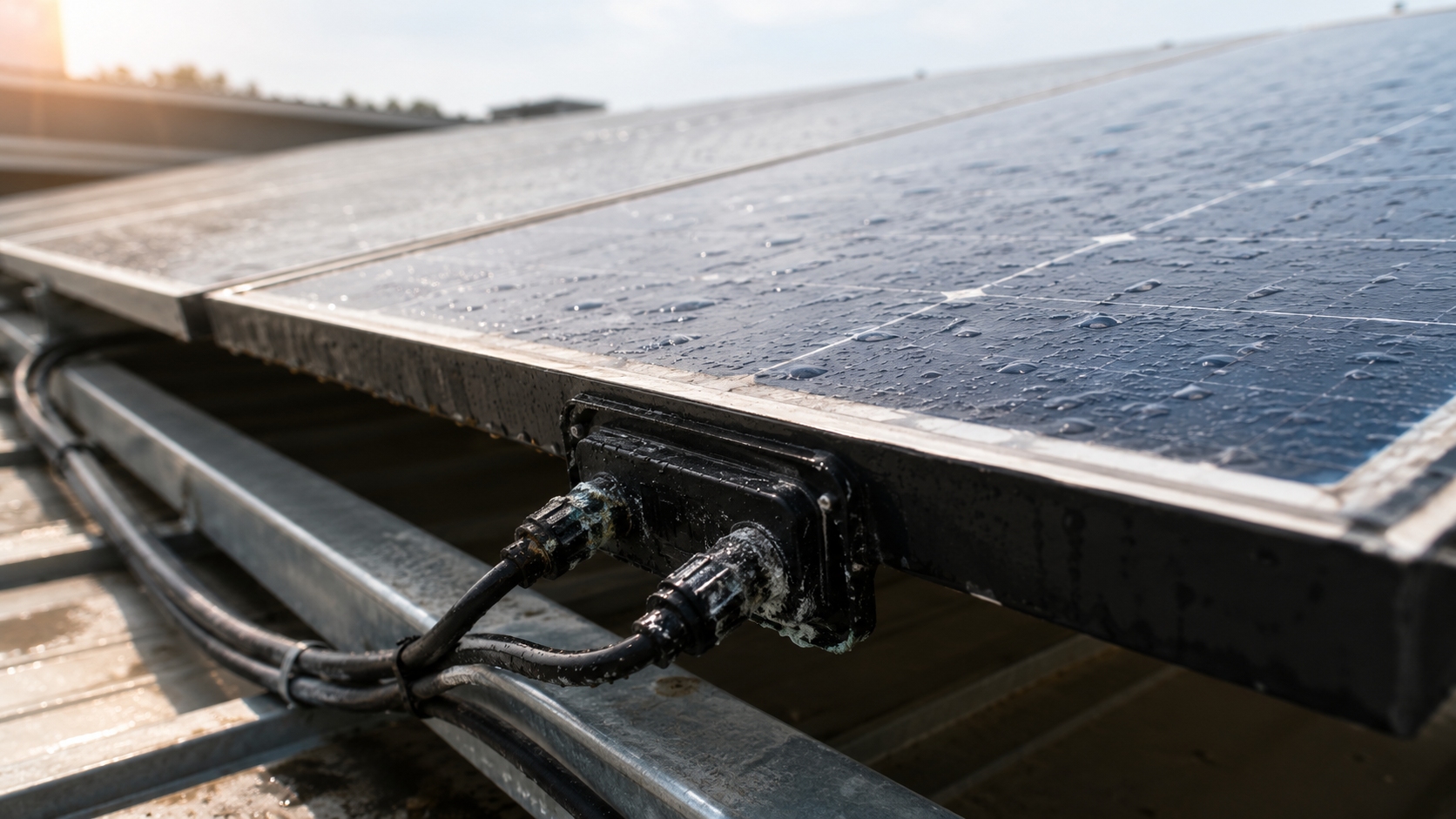
Tongwei's PV testing and R&D facilities include cell testing, materials analysis, module reliability testing, and failure analysis, illustrating the different types of evidence needed to move from an electrical symptom to a physical root cause.
Decide Whether the Device Actually Failed
The percentage increase can be misleading if it is separated from the absolute current and the product limit.
A rise from 1 nA to 5 nA is a 400% increase. The final 5 nA can still be far below the allowed limit.
A rise from 100 µA to 120 µA is only 20%, but it can matter more if 120 µA is close to the applicable limit.
| Result | Meaning |
|---|---|
| Within normal distribution and stable | Normal variation may explain the change |
| Still within limit but clearly shifted | Parametric degradation; investigate the trend |
| Above product or qualification limit | Specification failure |
Also avoid turning 85°C/85% RH test hours directly into field years. IEC 61215-1 states that PV module service life depends on design, environment, and operating conditions and that qualification testing is not a quantitative lifetime prediction.[12]
Fix the Confirmed Cause
| Confirmed Cause | Corrective Action |
|---|---|
| Ionic contamination | Review cleaning chemistry, rinsing, process water, flux, plating residue, and handling. |
| Fixture or PCB leakage | Correct socket cleanliness, PCB residue, cables, insulation, creepage, and measurement environment. |
| Passivation defect | Check film coverage, pinholes, adhesion, edge coverage, and surface preparation. |
| High-field edge leakage | Review termination design, field-control structures, local contamination, and passivation. |
| Delamination | Review material adhesion, surface preparation, cure or lamination conditions, and material compatibility. |
| Moisture ingress | Identify the shortest moisture path and improve the affected package, edge, encapsulant, or seal. |
| Corrosion or migration | Remove the contamination/moisture source and review metal, material, voltage, and interface conditions that enabled the reaction. |
Finally
Start with the measured current and work backward to the path that can physically carry it. At 600 V, a 1 GΩ unintended path already carries 0.6 µA; at 100 MΩ, the same voltage gives 6 µA. If a sample moves from 0.8 µA to 5.0 µA and returns to 1.1 µA after drying, moisture-dependent conduction explains most of the change. If the current stays high, keeps rising with stress time, or appears together with lower breakdown voltage, move the investigation toward passivation, junction edges, corrosion, migration, and moisture paths. Keep the test temperature, fixture, timing, and comparison method under control before calling the device itself defective.