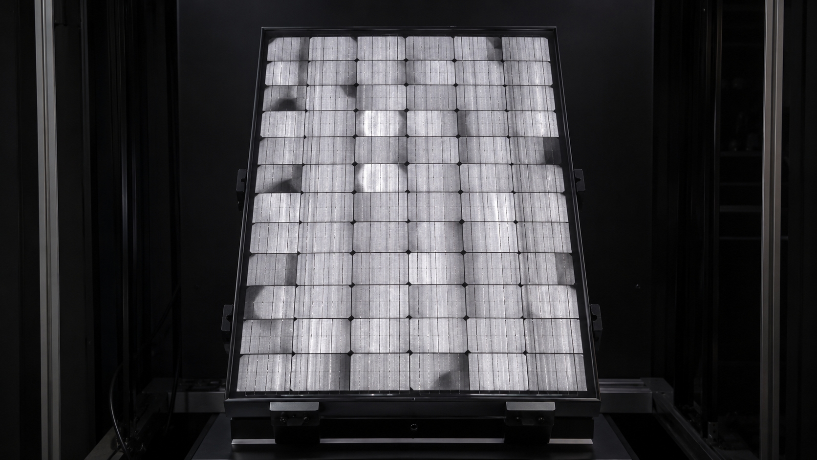
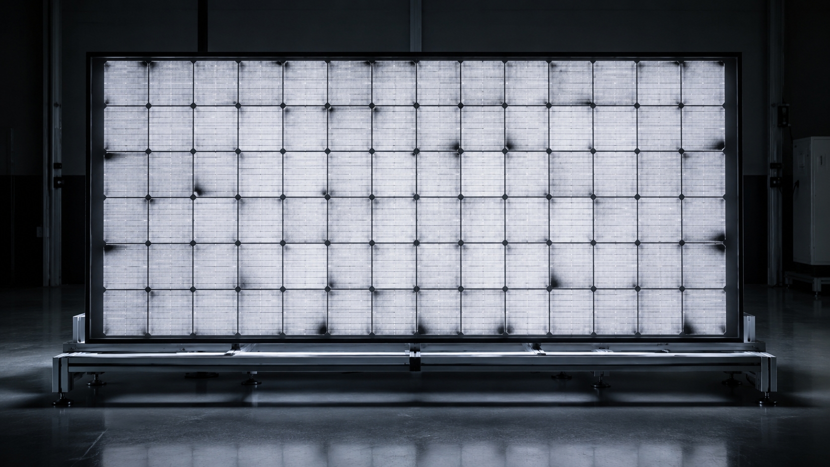
Dark cell corners usually come from an incomplete isolation line, damaged edge passivation, a resistive current path, cutting damage, or a crack that disconnects the corner. Check three things first: the shape of the dark boundary, how it changes between low and normal current, and the production stage at which it first appeared.
Read the Pattern
| EL pattern | First cause to check | Best confirming test |
|---|---|---|
| Smooth dark gradient toward the corner | Weak passivation, edge recombination, or distributed resistance | PL and two-current EL |
| Sharp triangular dark area | Crack or electrically disconnected corner | Magnified EL and microscopy |
| Straight dark border parallel to the edge | Isolation line placed too far inside the cell | Measure the groove position |
| Dark point where two isolation lines meet | Incomplete isolation or excessive laser overlap | Dark I-V, microscopy, and thermography |
| Much darker at low current | Leakage, shunting, or high recombination | Dark I-V and PL |
| Much darker at high current | Finger, contact, wire, solder, or TCO resistance | Multi-bias EL and infrared imaging |
| Pattern moves when the sample position changes | Lens shading, sensor response, or fixture shadow | Move the same corner to the center of the camera frame |
EL brightness is not a direct power measurement. Local voltage, recombination, resistance, temperature, and camera settings all change the recorded intensity. IEC TS 60904-13 covers EL capture and interpretation for forward-biased modules, while IEC TS 63202-2 applies to non-encapsulated crystalline-silicon cells.[1][2]
Check When It Appeared
| First appearance | Likely sources | Immediate check |
|---|---|---|
| After isolation | Open isolation path, groove offset, laser damage | Inspect both corner grooves |
| After metallization | Missing finger, poor print, metal-to-silicon contact | Compare with the pre-print image |
| After cutting | Unpassivated edge, rough cut, chip, microcrack | Compare before-and-after EL or PL |
| After stringing | Wire, ribbon, solder, or adhesive contact | Compare with the pre-string EL image |
| After lamination | Crack growth, local pressure, shifted interconnection | Compare pre- and post-lamination EL |
| After field use | Corrosion, solder fatigue, PID, mechanical loading | Check I-V, module position, and thermal image |
A bare solar cell can show defects from edge processing, printing, cutting, and test probes. A finished PV module adds glass, encapsulation, interconnection, lamination, moisture, and field-load variables.
Incomplete Isolation
Edge isolation must form one continuous electrical barrier. If two isolation lines do not meet at a corner, conductive material can still connect the front and rear regions.
Evidence that supports incomplete isolation:
- The dark area begins exactly where two isolation lines meet.
- The corner is more visible at low injection current.
- Shunt resistance is lower than that of approved cells.
- Dark I-V shows extra leakage.
- Thermography shows local heating at the groove junction.
Inspect the complete corner under magnification. A groove may look continuous from a normal viewing distance but still contain a small untreated gap, debris bridge, shallow section, or missed rounded edge.
Do not label the defect as poor passivation when the main electrical result is low shunt resistance. Passivation loss removes carriers; incomplete isolation creates an unwanted current path.
Excessive Isolation
An isolation line can block leakage correctly but still remove too much active cell area. This produces a regular dark border outside the groove.
The geometric effect can be calculated. For a simple 182 mm square cell:
| Isolation line moved inward | Remaining side length | Area removed | Share of square area |
|---|---|---|---|
| 0.2 mm on every side | 181.6 mm | 145.4 mm² | 0.44% |
| 0.5 mm on every side | 181.0 mm | 363.0 mm² | 1.10% |
| 1.0 mm on every side | 180.0 mm | 724.0 mm² | 2.19% |
These figures are area calculations, not power-loss values. Real cells have chamfers, metal coverage, existing inactive margins, and non-uniform current density. The calculation shows why a groove offset of only 0.2–0.5 mm should not be ignored.
Measure the groove-to-edge distance on both straight sides and at the corner. If the same wide border appears on cells from one laser tool or recipe, check alignment before investigating material quality.
Laser Damage
| Physical damage | Electrical result | EL evidence |
|---|---|---|
| Passivation layer removed | Higher edge recombination | Smooth dark gradient beside the groove |
| Junction exposed or damaged | Leakage and lower shunt resistance | Dark point or narrow band |
| Silicon melted and re-solidified | Recombination or unstable leakage | Irregular dark zone |
| Microcrack starts at the groove | Interrupted fingers or isolated area | Sharp line or triangular corner |
| Conductive debris remains | Local shunt | Small dark point with possible heating |
Check laser power, focus, scan speed, pulse overlap, and the scanner's movement at the corner. The effective energy can rise when the scanner slows or when two paths overlap.
EL identifies the damaged location but does not identify the incorrect machine setting. Match the image with groove width, surface microscopy, and equipment records.
Passivation Loss
Weak passivation increases carrier loss at the edge without necessarily producing a low-resistance short circuit.
Check for:
- Thin or incomplete dielectric coverage
- Pinholes
- Contamination before coating
- Poor cleaning
- Scratches and edge chips
- Laser removal of the coating
- Newly exposed silicon after cutting
Use EL and PL together:
| Image result | More likely cause |
|---|---|
| Dark in EL, more uniform in PL | Current delivery, finger, contact, or interconnection fault |
| Dark in both EL and PL | Passivation loss, high recombination, material damage, or optical attenuation |
| Dark in EL beyond a crack, but visible in PL | Electrical isolation without equal material-quality loss |
Normal shunt resistance does not rule out poor passivation. A passivation defect can lower local carrier density and voltage while the dark I-V curve remains free of a strong leakage path.
Cut-Edge Damage
Cut cells have more exposed edge length relative to active area. Half cells, narrow rectangular cells, and shingle strips are therefore more sensitive to cutting quality than full cells.
A 2024 study of industrial heterojunction cells reported the following edge-recombination values at the stated carrier condition:
| Edge condition | Surface recombination velocity | Relative to native edge |
|---|---|---|
| Native edge | About 250 cm/s | 1× |
| Thermal-laser-separated edge | About 750 cm/s | 3× |
| Laser-scribed edge | About 11,000 cm/s | 44× |
The laser-scribed edge was about 14.7 times the thermal-laser-separated value. The study also estimated efficiency losses of approximately 0.1 percentage point for the native full-cell edge, 0.3 point for a thermal-laser-separated half cell, and 1.1 points for a shingle strip under its test and simulation conditions.[3]
These values are not universal production limits. They show that a rough or heavily damaged cut edge can increase carrier loss by more than one order of magnitude.
Use this check:
- Capture EL or PL before cutting.
- Repeat the image after cutting with the same current, exposure, focus, and temperature.
- Check whether a new dark band follows the new edge.
- Inspect the edge for chips, roughness, scribe damage, and cracks.
- Compare voltage and fill factor before and after cutting.
Research comparing PERC and heterojunction cells found that much of the separation loss came from the newly exposed unpassivated edge rather than from the thermal cleaving action alone.[4]
Two-Current Test
A useful approach is to compare a lower-current image with an image near the normal production EL current. For example, 0.2 × Isc and 1.0 × Isc may be used when both are safe for the sample and equipment. These are illustrative test levels, not universal acceptance limits.
| Result | First fault to check |
|---|---|
| Dark at 0.2 × Isc, less different at 1.0 × Isc | Shunting, leakage, or edge recombination |
| Near normal at 0.2 × Isc, darker at 1.0 × Isc | Finger, contact, wire, solder, adhesive, or TCO resistance |
| Sharp region remains almost black at both currents | Fully or partly disconnected area |
Module EL is commonly performed using forward current near the module's short-circuit current under standard test conditions. Lower-current imaging is used to expose bias-dependent defects.[5]
Keep exposure, gain, aperture, focus, position, temperature, electrical contact, and capture delay controlled. Do not compare a cold low-current image with a heated normal-current image.
Resistance Loss
A simple example shows why a small added resistance can create clear EL contrast:
| Local current | Added local resistance | Voltage loss |
|---|---|---|
| 5 A | 5 mΩ | 25 mV |
| 10 A | 5 mΩ | 50 mV |
| 15 A | 5 mΩ | 75 mV |
The calculation follows voltage loss = current × resistance. A real cell is a distributed network, so the terminal current cannot simply be assigned to one corner. Quantitative resistance mapping requires corrected images, voltage calibration, and an electrical model.[6]
Check these current paths separately:
- Lateral current through the emitter or transparent conductive oxide
- Transfer from the semiconductor into the metal contact
- Current along the metal finger
- Transfer into a wire, ribbon, solder joint, or conductive adhesive
A finger may look complete while the contact below it is poor. A broken finger may also remain partly active because current can move sideways to another finger. Both faults can create a smooth corner gradient rather than a completely black area.
Interconnection design changes the pattern. Multi-wire and 0BB structures use more current-transfer points than older wide-busbar layouts. The expected normal EL pattern should be set for each module design, not copied from another product.
Crack Evidence
| Crack state | EL result | Electrical meaning |
|---|---|---|
| Connected | Crack line visible, surrounding area still bright | Enough current paths remain |
| Partly isolated | Corner is dark but not black | Some fingers are interrupted |
| Fully isolated | Sharp black triangle or fragment | Little current reaches the area |
| Intermittent | Contrast changes with load or temperature | Crack faces open and close |
A triangular dark corner with a 20 mm base and 25 mm height has an image area of:
20 mm × 25 mm ÷ 2 = 250 mm²
A simple 182 mm square has an area of 33,124 mm², so the triangle represents approximately 0.75% of the square area. It does not prove 0.75% power loss. The result depends on how many fingers are cut and whether current can still enter the region.
A study of 230 mini-modules using full-cell PERC and half-cut TOPCon cells found that crack count and crack length alone did not consistently predict power loss. Busbar count, cell structure, and irradiance changed the result. The study examined line cracks that had not formed electrically isolated cell areas, so its conclusion does not apply directly to a fully disconnected black triangle.[7]
PID and Corrosion
PID should move high on the fault list only when several pieces of evidence agree:
- Several cells or modules show a related edge pattern.
- The pattern follows module position within a high-voltage string.
- Shunt resistance, voltage, or fill factor has changed.
- The module has a suitable voltage, temperature, and moisture history.
- Controlled recovery or PID testing changes the result.
PID-s mainly creates shunting, PID-p mainly affects polarization or passivation, and PID-c involves corrosion-related damage. Their EL and I-V patterns are not identical.[8]
A single isolated dark corner without a string-voltage pattern is weak evidence for PID.
Moisture-related dark edges should also be checked for metal and contact corrosion. In one damp-heat study, samples were exposed to 80% relative humidity at 80°C or 90°C for up to 2,500 hours. The dark edge regions showed increased series resistance, while internal quantum-efficiency results did not show a matching increase in junction recombination. Grid corrosion was identified as the more likely cause.[9]
Accelerated test hours do not equal a fixed number of outdoor years. Qualification and reliability tests must be read with their intended purpose and limitations in mind.