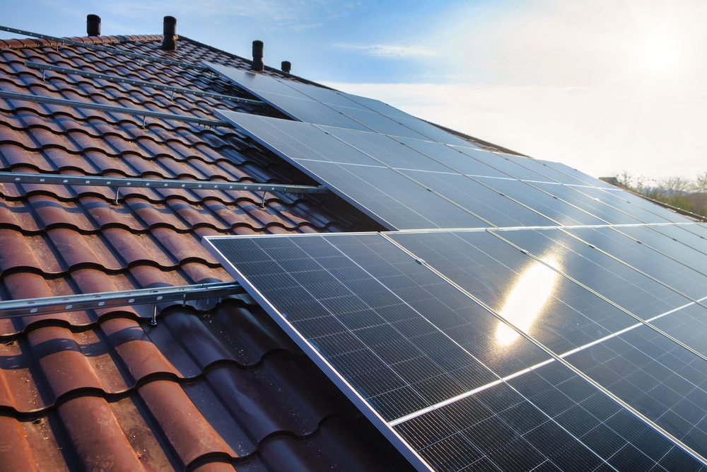
Why Small Solar Modules Fail | 5 Common Mistakes
The failure of small-scale modules stems from poor encapsulation inducing PID effects that cause a 30% power drop, as well as solder joint micro-cracks and diode defects that generate hot spots exceeding 100°C during shading, leading to a lifespan reduction of over 50%.
Moisture Ingress
Water vapor penetrates through the encapsulation materials, triggering electrochemical oxidation during 85°C/85% Damp Heat (DH) testing.
The Water Vapor Transmission Rate (WVTR) of standard EVA is approximately 30g/m²/day. If sealing is inadequate, the series resistance can rise by more than 20% within 6 months.
Switching to POE materials or edge butyl rubber can reduce the permeability to below 1 g, maintaining a power output of over 98%.
Differences in Permeability
The encapsulation layer typically consists of polymer materials with a thickness of 450 to 600 microns. The most common ethylene-vinyl acetate (EVA) on the market generally has a water vapor transmission rate between 30 and 50 g/m²/day under standard test conditions of 38°C and 90% relative humidity.
In contrast, Polyolefin Elastomer (POE), due to its non-polar molecular structure, has a water vapor transmission rate of only 2 to 5 g/m²/day at the same thickness.
This difference of more than tenfold in performance becomes very apparent during long-term outdoor operation.
Small modules have a wide range of applications, such as streetlights, meteorological monitors, or portable charging devices, and their Perimeter-to-Area Ratio is much higher than that of large-scale power station modules.
The path for water vapor to penetrate the internal circuits from the side cuts is shorter and the speed is faster.
If high-permeability EVA materials are used without effective edge blocking, moisture will reach the light-receiving surface of the cells through diffusion within 12 months, triggering electrochemical corrosion of the silver paste grid lines.
Material Physical Property Comparison | Density (g/cm³) | Volume Resistivity (Ω·cm) | WVTR (g/m²/day) | Cross-linking Standard (%) |
Standard EVA Film | 0.95 | 10^14 | 35.5 | 75 - 85 |
Enhanced POE Film | 0.88 | 10^16 | 3.2 | 60 - 70 |
Co-extruded EPE (EVA/POE/EVA) | 0.92 | 10^15 | 12.8 | 70 - 80 |
PVDF Back sheet | 1.78 | 10^13 | 1.5 | N/A |
On a microscopic scale, water vapor enters the encapsulation layer in two ways: Bulk Diffusion and Interfacial Diffusion. Bulk diffusion depends on the size of the gaps between polymer chains, while interfacial diffusion occurs at the contact surfaces between the cells, ribbons, and the film.
Many low-cost small panels use PET (Polyethylene Terephthalate) as a single-layer backsheet, which is typically only 150 to 200 microns thick.
Although PET material itself has a certain level of mechanical strength, its hydrolysis resistance is weak. In high-temperature and high-humidity environments, water molecules break the polyester chains, causing the material to become brittle and develop micro-cracks.
Once micro-cracks form, external moisture invades the interior through these channels at a geometric rate.
High-end off-grid modules choose fluoropolymer composite backsheets (such as TPT or TPE structures), which contain a 25-micron thick Polyvinyl Fluoride (PVF) or Polyvinylidene Fluoride (PVDF) layer, controlling the overall module's water vapor transmission rate to below 1.0 g/m²/day.
This material combination ensures that the power attenuation of the internal cells is controlled within 3% after 2000 hours of Damp Heat testing (DH2000).
Furthermore, the anti-reflective coating (SiNx) on the front of the cells undergoes chemical degradation when it comes into contact with the acidic moisture that has penetrated, causing the surface passivation effect to fail, which manifests as a significant drop in short-circuit current (Isc).
During the manufacturing process of small modules, uneven pressure distribution in the laminator can lead to thinning of the film in the edge areas, with some parts even being compressed from 500 microns down to 200 microns.
This inconsistency in physical thickness leads to localized weakening of penetration resistance.
Moisture tends to cut in from these weak points and spread toward the center along the gaps of the busbars.
Experimental data shows that at 85°C and 85% humidity, the diffusion coefficient of water molecules in EVA is approximately 10^-7 cm²/s.
For a small module with a width of only 100 mm, it takes less than two years for moisture to penetrate from the edge to the center.
If lead-containing solder is used for the ribbons, the combination of moisture and acidic substances (such as acetic acid produced by EVA hydrolysis) will form lead acetate salts. These white or gray spots block the current paths, causing the series resistance (Rs) to rise by 30% to 50% in the short term.
Acetic Acid Reaction
When moisture penetrates the encapsulation layer, the vinyl acetate groups in the EVA molecular chains undergo a hydrolysis reaction, releasing free acetic acid molecules.
At room temperature, this chemical reaction is slow, but when the module surface temperature rises to 60°C to 85°C due to sunlight, the hydrolysis rate increases exponentially.
Laboratory data indicates that in a standard damp heat test (DH85/85) environment, after 1000 hours of exposure, the concentration of acetic acid generated by hydrolysis can accumulate to 2000 ppm to 5000 ppm.
Since small modules often use thinner backsheets or simplified edge encapsulation processes, acetic acid cannot be slowly discharged through "breathing" as it is in large modules; instead, it continuously accumulates at the interface between the cells and the glass.
The acidic substance reacts chemically with the silver grid lines on the cell surface to generate silver acetate.
This reaction causes the metal structure of the grid lines to become loose, significantly reducing electrical conductivity.
Damp Heat Exposure Time (Hours) | Estimated Internal Acetic Acid Conc. (ppm) | Series Resistance (Rs) Change Rate (%) | Power Attenuation (Pmax) (%) |
0 | 0 | 0.0 | 0.0 |
500 | 1200 | 8.5 | 2.1 |
1000 | 3500 | 22.4 | 6.8 |
2000 | 7800 | 55.0 | 18.5 |
The acetic acid reaction is not limited to destroying conductive grid lines; its corrosion of the ribbons is equally destructive.
The ribbons used in small modules typically consist of a copper core coated with a tin-lead alloy (Sn-Pb).
Acetic acid preferentially attacks the tin-lead layer, producing lead acetate and other salts.
This corrosion product typically appears as a white powdery accumulation distributed in the contact area between the ribbon and the cell.
As the depth of corrosion increases, the ohmic contact between the ribbon and the cell gradually fails, causing internal resistance to climb from an initial 0.2 ohms to over 1.5 ohms.
· Formation of Acidic Electrolyte: Accumulated acetic acid combines with penetrated moisture to create a low-pH, weakly acidic electrolytic environment inside the module.
· AR Coating Erosion: The Silicon Nitride (SiNx) anti-reflection layer on the cell surface gradually thins in an acidic environment, weakening the surface passivation effect and increasing the recombination rate of photogenerated carriers.
· Leaching of Alkaline Substances from Glass: Acetic acid exchanges with sodium ions (Na+) in the soda-lime glass, resulting in cloud-like etching on the glass surface and a drop in light transmittance of about 2% to 5%.
· Acceleration of Charge Migration: Acidic ions increase the conductivity of the encapsulation material, making it easier to induce Potential Induced Degradation (PID) when a system potential difference exists.
Physical delamination often accompanies the intensification of the acetic acid reaction. The adhesion of the EVA film to the cell surface primarily relies on chemical bonds formed by silane coupling agents. Acidic substances hydrolyze these coupling agent molecules, causing the peel strength to drop sharply from a standard 60 N/cm to below 5 N/cm.
The chemical structure of POE consists of saturated carbon chains. Even when exposed to extreme environments of 85°C and 85% humidity for 3,000 hours, it does not produce any acidic byproducts, and the internal pH remains neutral at around 7.
For scenarios where EVA must be used, adding acid-absorbing additives or using high-barrier co-extruded EPE materials (EVA-POE-EVA structure) can slow down the accumulation rate of acetic acid concentration.
Experimental comparisons show that the endurance of small modules using EPE material in the same environment is approximately 2.5 times longer than that of pure EVA modules.
As the concentration of acetic acid increases, the EVA polymer chains break and re-crosslink, causing the material's absorption spectrum to shift toward shorter wavelengths.
This phenomenon manifests visually as yellowing or brown spots around the module edges or ribbons.
The loss of light transmittance leads to a reduction in the number of photons reaching the cell surface, resulting in a trend of declining short-circuit current (Isc).
In tropical regions, this acetic acid-induced yellowing process typically becomes very significant by the 24th to 36th month of product use, ultimately making the product's energy output far lower than the design expectations.
Poor Junction Box Design
Junction box failures account for over 15% of field failures in small-scale modules.
Low-cost designs often adopt an IP54 protection rating, which has a water vapor transmission rate more than 200% higher than the IP67 standard in long-term outdoor testing.
If internal Schottky diodes lack effective heat dissipation space, their junction temperature can exceed the 125°C rating threshold when the ambient temperature is 35°C, leading to increased leakage current.
If the contact resistance at electrical connections is higher than 5 milliohms, it will directly cause power loss and localized heating.
Material Anti-Aging Levels
Most cheap modules with rated power between 10W and 80W often improperly use ABS (Acrylonitrile Butadiene Styrene) or unmodified PC (Polycarbonate) plastic to save approximately $0.50 in production costs.
The relative temperature index (RTI) of these materials is typically only 60°C to 80°C, far below the 105°C standard required by the international electrical standard UL 3730 for junction boxes.
In tropical regions or high-radiation summer environments, the backsheet temperature of the module can easily reach over 75°C, at which point low-end materials undergo thermal degradation of their molecular chains.
According to ASTM G155 cycle test data, the notched impact strength of ABS material drops by more than 75% after receiving a total UV dose of 1000 MJ/m².
This degradation manifests macroscopically as yellowing and microscopically as polymer cracking.
As flexibility is lost, the material becomes as brittle as a biscuit, and貫穿性 physical cracks occur in the housing when encountering hail, wind-driven cable swaying, or tugging during routine maintenance.
Moisture penetrates into the electrical chamber through these micron-level cracks, causing the insulation resistance between the internal busbars and the external environment to drop rapidly from over 400 MΩ to less than 10 MΩ, ultimately triggering the system's leakage protection trip.
Physical Property Parameters | Modified PPO Standard | Cheap ABS Plastic Actual Performance | Test Standard Reference |
Relative Temperature Index (RTI) | 105°C to 110°C | 60°C to 75°C | UL 746B |
Water Absorption (24h/23C) | Below 0.06% | Above 0.30% | ISO 62 |
Flame Retardancy (3.0mm thickness) | UL94-V0 (Self-extinguishing) | UL94-HB (Continuous burning) | UL 94 |
Tensile Strength Retention (3000h UV) | Above 90% | Below 25% | ASTM D638 |
Dielectric Strength | 30 kV/mm | 15 kV/mm | IEC 60243 |
In the 85/85 damp heat test required by the IEC 62790 standard, after 1000 hours of continuous operation, the fluctuation in tensile strength for high-quality PPO material is less than 5%.
In contrast, low-quality plastics undergo physical expansion in high-temperature and high-humidity environments, with water absorption rates as high as 0.3% or more.
Since small modules often use simple manual gluing processes, the sealant at the bonding interface will undergo cohesive failure or interfacial detachment under the repeated pulling of material thermal expansion and contraction.
Laboratory data shows that after 200 thermal cycles, the peel strength of poor-quality junction boxes drops from an initial 40 N/cm to less than 12 N/cm.
Environmental Simulation Test Item | PPO Material Appearance & Performance Changes | ABS/Non-standard PC Appearance & Performance Changes |
1,000 h Xenon Arc UV Aging | Slight loss of gloss, no visible cracks | Severe yellowing, spider-web micro-cracks |
-40 to +85°C Thermal Cycling | Dimensional change <0.1%, no deformation | Significant distortion, screw threads stripping |
High-intensity Salt Spray (96 h) | No internal oxidation, stable insulation | Salt penetration, green verdigris on terminals |
Ball Impact Test (2 kg/1 m) | Slight surface scratches, intact structure | Brittle shell fracture, fragments falling off |
In agricultural irrigation systems or livestock monitoring applications, ammonia and fertilizer volatiles in the air can trigger stress cracking reactions with specific plastics.
Qualified junction box materials must pass various chemical reagent immersion tests to ensure their inertness.
High-quality PPO material maintains a stable molecular weight distribution when in contact with nitrogenous compounds or weakly acidic rainwater, whereas inferior PC/ABS blends rapidly release internal stresses under these chemical factors, manifesting as spontaneous cracking around the mounting holes of the junction box.
Furthermore, the selection of flame retardants also determines the long-term stability of the material.
Cheap products often use bromine-containing flame retardants, which decompose under UV radiation and release acidic gases that corrode the circuit from the inside.
In contrast, halogen-free flame-retardant PPO, which complies with mainstream international environmental standards, avoids this endogenous destruction.
For small off-grid systems deployed near the ocean or in high-humidity zones, the rate at which the material's volume resistivity decays over time determines the overall safety of the system.
After five years of operation, the dielectric constant of poor materials increases due to moisture absorption, causing charges to accumulate easily on the housing surface, which not only increases the risk of electric shock for maintenance personnel but also greatly increases the probability of electrostatic discharge (ESD) damaging internal bypass diodes.
Choosing weather-resistant materials with UL certification and complete data sheet support is a fundamental engineering requirement to avoid early failure of small modules and ensure a design life of over 20 years.
Internal Thermal Management
Taking a 100W module with a rated current of 8 amps as an example, when using standard Schottky diodes, the forward voltage drop is usually around 0.55 volts.
When the module is shaded and the diode conducts, the thermal power generated by a single device is approximately 4.4 watts.
In a completely sealed plastic box with a volume of about 40 cubic centimeters, if heat is not discharged through conduction or convection, the internal air temperature will rise significantly in a short time.
Test data shows that under conditions of 35°C ambient temperature and 1,000 W/m² irradiance, the internal equilibrium temperature of junction boxes lacking heat dissipation design often exceeds 90°C.
The diode junction temperature at this point approaches the physical limit of 150°C, causing degradation of the semiconductor material's electrical performance.
The reverse leakage current of a diode is exponentially related to temperature. For every 10°C increase in temperature, the reverse leakage current approximately doubles.
For small modules, if internal heat accumulation keeps the diode in an environment above 85°C for a long time, its internal Schottky barrier will suffer physical damage, causing the leakage current to rise from microamps to milliamps.
The result is that the diode consumes power even in the non-conducting state and generates further heat. This phenomenon is known as thermal runaway.
In extreme cases, thermal runaway can cause the internal temperature of the junction box to soar to 200°C within minutes, leading to the housing melting or the backsheet burning.
Heat Dissipation Solution | Thermal Conductivity (W/mK) | Junction Temp Rise (Above Ambient) | Expected Service Life (Years) |
Natural Air Convection (No Potting) | 0.026 | 55 - 75°C | 2 - 5 |
Epoxy Potting | 0.20 - 0.35 | 30 - 45°C | 8 - 12 |
Silicone Thermal Sealant | 0.80 - 2.50 | 15 - 25°C | 15 - 25 |
Ceramic Substrate Heat Sink | 20.0 - 35.0 | 5 - 12°C | 25+ |
The circuit layout of small modules is often too crowded, with the distance between diode pins and metal busbar solder points being too short.
Heat conducts rapidly along the metal conductor to the solar cells.
Since the power output of solar cells has a negative temperature coefficient, for every 1°C increase in local temperature, the output power drops by about 0.4%.
Thermal feedback from the junction box area causes hot spots in the cells near the box.
This long-term high-temperature environment accelerates the decomposition of the encapsulation material EVA, releasing acetic acid, which in turn corrodes the cell's silver grid lines and ribbons, causing the module's internal resistance to increase by over 30% within 3 to 5 years.
Internal thermal management also involves the calculation of the thermal resistance chain.
From the diode chip to the pins, from the pins to the internal air of the junction box, and finally through the housing to the external environment, obstacles to heat discharge exist at every layer.
For the small junction boxes of 5W to 50W modules, external wind speed has a negligible effect on cooling. Effective thermal management relies on the thermal conductivity of the internal filling material.
· Filling Rate Requirement: Potting material must completely cover diode pins and metal connection plates, filling over 90% of the box space to reduce air gaps.
· Diode Redundancy: When selecting diodes, the rated current should be at least 1.5 to 2 times the module's short-circuit current (Isc) to reduce the current density of the single device.
· Physical Gap: The diode body should maintain an air gap of at least 5 mm from the bottom backsheet or be mounted with a thermal silicone pad to prevent localized heat accumulation.
· Busbar Width: Increase the cross-sectional area of the busbars inside the junction box to utilize copper's good thermal conductivity as a temporary heat sink.
Diode Working State | Internal Temp (No Dissipation) | Internal Temp (With Thermal Glue) | Impact on Module Power |
100% Power Output (No Shading) | 45°C | 38°C | Normal Operation |
50% Area Shaded (Continuous Conduction) | 115°C | 62°C | Long-term EVA yellowing |
Short Circuit Test (2 h Duration) | 145°C | 78°C | Potential insulation thermal failure |
The Heat Deflection Temperature (HDT) of the junction box material also limits the upper boundary of internal thermal management.
If cheap plastic with an HDT of only 80°C is used, the housing will undergo creep due to internal air pressure and high temperature even if the diode itself can withstand high heat.
The result is loose cable glands, losing the original IP67 protection rating.
In environments with frequent high-low temperature alternation in the wild, the frequent expansion and contraction caused by heat will cause metal fatigue in internal solder joints.
According to fatigue life estimations, if the operating temperature difference expands from 30°C to 60°C, the cyclic life of the solder joints will be shortened to one-fourth of the original.
High-performance small modules are designed with reference to the IEC 62,790 standard for rigorous thermal cycling and bypass diode thermal performance testing.
In tests, modules are required to have 1.25 times the short-circuit current passed through them for one hour at a baseline of 75°C, and the maximum temperature of the junction box housing must not exceed the material's RTI.
If the air circulation path inside the junction box is blocked, or if the diode layout is too concentrated, localized heat accumulation will trigger thermoplastic deformation of the housing surface.
For small systems installed on roofs or in enclosed brackets, the internal thermal management pressure increases by an additional 20% to 30% due to the lack of rear airflow.
Voltage Mismatch
Small panels with a nominal 12V rating require an operating voltage (Vmp) of around 18V to offset line losses and meet the 14.4V charging requirement.
If the difference between Vmp and the cell voltage is less than 2V, charging efficiency will drop by more than 40%.
Simultaneously, if the open-circuit voltage (Voc) after connecting multiple panels in series exceeds the controller's rated value (e.g., 100 V), it will directly burn out the internal circuits.
For every 1°C change in ambient temperature, the voltage fluctuates by about 0.3%, which is the technical reason for system shutdowns in extreme weather.
Charging Voltage Difference
For common nominal 12V systems, the Vmp of a single solar panel is usually set between 17.5V and 19V, while cell voltage during charging cycles typically fluctuates from 10.5V to 14.8V.
This 3V to 5V voltage redundancy is not wasted; it is used to offset multiple voltage losses throughout the circuit.
When light intensity drops to 200 W/m², the panel output voltage shrinks significantly. If the initial designed voltage difference is too small, the current will be unable to overcome the cell's electromotive force to enter the internal resistance.
For example, when the ambient temperature rises to 65°C, the voltage of the photovoltaic module will drop by about 12% according to the negative temperature coefficient (usually -0.3%/°C). An 18V panel will drop to around 15.8V, which, after deducting line losses, just maintains the 14.4V absorption charging voltage.
If a panel with an operating voltage of only 16 V is chosen, the potential difference will completely disappear, causing the system to stop charging at noon on a sunny day.
The table below shows the voltage drop generated by copper wires of different lengths and gauges (AWG standard) at a 10A current, which directly consumes the charging voltage difference space:
Wire Gauge (AWG) | Wire Length (Feet) | Voltage Drop (Volts) | Impact on 12V System ΔV (%) |
14 AWG | 10 | 0.52V | Approx. 3.6% |
12 AWG | 20 | 0.65V | Approx. 4.5% |
10 AWG | 25 | 0.51V | Approx. 3.5% |
16 AWG | 15 | 1.22V | Approx. 8.5% |
Taking a LiFePO4 (Lithium Iron Phosphate) cell as an example, its charge-discharge curve is extremely flat, with single-cell voltage maintained at 3.2V to 3.3V for long periods. A 12.8V cell pack made of four cells in series requires 14.2V to 14.6V at the end of the charging phase (absorption stage).
If the combination of solar panel and controller cannot provide an output exceeding 15 V, the current will decrease rapidly due to insufficient potential difference, resulting in the cell remaining uncharged for a long time, leading to a decline in internal chemical activity.
In actual installations, if a PWM controller is used, the panel voltage is forced down to near the cell voltage, and the excess voltage difference is converted into heat loss.
When using an MPPT controller, the existence of a voltage difference allows the controller to convert high-voltage low-current into low-voltage high-current through a converter.
For example, 36V/5A (180W) power at the input can achieve efficient charging of 14.4V/12.5A at the output, provided the input voltage is at least 2V to 5V above the cell voltage as a starting threshold.
A 100Ah lead-acid cell may have an internal voltage drop of 0.2V to 0.4V at a discharge current of 20A, making the cell's external terminal voltage appear lower than the actual internal electromotive force.
During charging, the panel must provide a higher voltage than the theoretical value to overcome this resistance barrier.
If the difference between the module's Voc (Open Circuit Voltage) and the load operating voltage is insufficient, the system will exhibit extremely poor stability in the face of voltage fluctuations caused by cloudy weather or partial shading.
The table below lists the minimum required voltage difference data for different charging stages (based on a 25°C standard environment):
Charging Stage | Cell Target Voltage (V) | Panel Min. Input Voltage (V) | Required Voltage Redundancy (V) |
Bulk Charge | 12.6V - 13.8V | 15.5V | 1.7V - 2.9V |
Absorption Charge | 14.4V - 14.8V | 17.5V | 2.7V - 3.1V |
Float Stage | 13.2V - 13.6V | 15.0V | 1.4V - 1.8V |
Equalization Stage | 15.5V - 16.0V | 18.5V | 2.5V - 3.0V |
In small portable photovoltaic devices, the voltage drop after heating is more severe than in industrial-grade modules due to the use of thin encapsulation materials and poor heat dissipation.
If the number of cells in series is reduced to pursue miniaturization, the panel's Vmp will drop to around 15V.
While this design may be feasible in a laboratory environment, in actual use, once the ambient temperature rises above 40°C, the panel surface temperature can reach 70°C, and the voltage will drop below 13 V.
Since the panel voltage is now lower than the 14.4V required to fully charge the cell, the charging current will approach zero.
Additionally, blocking diodes used in the system typically generate a constant voltage drop of 0.4V to 0.7V, and connector contact resistance at high currents also consumes about 0.1V of the voltage difference.
These seemingly small values add up, quickly exhausting a tight voltage difference budget and causing energy transmission efficiency to drop by more than 30%.
For systems with off-grid designs, when considering wiring lengths of over 20 feet, the voltage drop loss must be compensated by increasing the nominal system voltage or the wire cross-sectional area.
If the system voltage is upgraded from 12V to 24V, the current is halved for the same power, and according to the voltage drop formula, the pressure loss on the wire will be reduced by 75%, leaving a wider margin for voltage matching between the module and the cell.
About 40% of small solar panel failure cases are attributed to an insufficient voltage difference that prevents the system from starting in the early morning, evening, or high-temperature conditions.
By choosing modules with higher voltage redundancy (e.g., a 12V panel with a Vmp of 20V), daily effective charging time can be significantly extended, improving the system's survival capability in non-ideal lighting conditions.
Controller Voltage Endurance
Every power semiconductor device inside a solar controller, such as MOSFETs or capacitors, is labeled with a maximum operating voltage rating.
In small off-grid systems, if the total open-circuit voltage of the modules in series exceeds the controller's rated input, even by just 1 volt, it can lead to internal module breakdown.
This damage manifests as the semiconductor layer losing its insulation capability, causing current to surge uncontrollably, generating high heat and burning the circuit board.
Controllers typically labeled as 100V often have an actual physical breakdown limit between 105V and 110V, leaving no redundancy to handle unexpected voltage fluctuations.
The table below lists the real voltage values that a standard solar panel with an open-circuit voltage of 45 V may reach in actual operation at different ambient temperatures:
Ambient Temp (°C) | Voltage Change Percentage | Single Panel Actual Voltage (V) | Two Panels Series Total (V) |
25°C (STC) | 0% | 45.0V | 90.0V |
10°C | Rise 4.5% | 47.0V | 94.0V |
0°C | Rise 7.5% | 48.4V | 96.8V |
-10°C | Rise 10.5% | 49.7V | 99.4V |
-20°C | Rise 13.5% | 51.1V | 102.2V |
If two 45V nominal panels are connected in series to a controller with a maximum 100V endurance, it will perform normally at 25°C with a total of 90V, but when the temperature drops below -10°C, the total voltage will climb above 100V.
If a voltage margin of about 20% is not reserved during design, hardware damage usually occurs on the first cold morning after sunrise.
When sunlight hits the freezing panels, the voltage instantaneously peaks. If the controller starts its self-check at this moment, the high-voltage current directly hits the input capacitors, resulting in hardware failure.
For controllers of different voltage classes, the following safety configuration suggestions can be referenced when designing small systems:
· 75V Rated Controller: A maximum of 2 nominal 12V panels (Voc ~22V) can be series-connected; if using 24V panels (Voc ~45V), only 1 is recommended.
· 100V Rated Controller: Supports 2 series-connected 24V panels, but in extremely cold regions (below -20°C), parallel mode is suggested instead.
· 150V Rated Controller: Allows 3 series-connected 24V panels; total voltage is 135V under standard conditions, leaving 15V for thermal drift.
· 250V Rated Controller: Mostly used for 48V systems or long-distance wiring, supporting 5 panels in series to effectively reduce line current losses.
MPPT controllers integrate complex buck-converter circuits whose inductors and switches are extremely sensitive to overvoltage.
Once the input voltage exceeds limits, control algorithms may not adjust the duty cycle in time, causing voltage to load directly onto the low-voltage side.
PWM controllers, while simpler in structure, also have fixed voltage ratings for their switches.
When the panel voltage is too high, PWM controllers cannot perform voltage conversion and will simply connect the panel directly to the cell, subjecting the cell to abnormally high voltage, which damages the controller and can lead to cell overcharging.
The table below summarizes the specific physical impacts of exceeding voltage limits on the controller and system modules:
Affected Module | Physical Reaction Description | Damage Probability & Consequence |
Input Electrolytic Capacitor | Electrolyte thermal expansion or puncture | Extremely High; manifests as capacitor bursting |
Switching MOSFET | Permanent conduction of semiconductor channel | High; causes controller to lose current cutoff ability |
Control Chip (MCU) | Encountering high-voltage reverse shock | Medium; leads to logic confusion or total death |
Sampling Resistor | Overcurrent/overheating causing resistance drift | Low; results in incorrect voltage display readings |
In small DIY systems, users tend to increase the number of series-connected modules to raise voltage and reduce current to save on wire costs.
However, this practice directly increases the voltage risk for the controller. If using a nominal 48V cell pack, at least two 24V panels are usually needed in series, at which point the Voc is already close to 90V.
If the chosen controller has an endurance of only 100 V, the system's operational stability in winter will drop to extremely low levels.
According to the National Electrical Code (NEC) recommendations, a correction factor of 1.25 should be used when calculating maximum system voltage.
If a panel's Voc is 40V, it should be treated as 50V when configuring the controller.
In addition to temperature effects, the cloud-edge effect can push light intensity above 1,200 W/m² for short periods.
In this case, the panel's output voltage and current will simultaneously exceed rated values.
Although the duration is short, for cheap controllers without overvoltage clamping protection, this instantaneous high-voltage surge is enough to puncture internal logic circuits.
Ensuring the controller has an automatic overvoltage protection (OVP) function with auto-recovery is an effective way to reduce failure risks.
When performing wiring operations, the cell must be connected before the solar panels to ensure the controller's internal logic units establish a working potential beforehand.
Shading & Hot Spots
Shading 10% of the cell area often leads to a drop in module output of over 50%.
Small modules, due to high internal resistance and a lack of multi-stage bypass diodes, turn shaded cells from power sources into loads, entering a reverse-bias state and forcibly consuming current generated by other cells.
Experimental data shows that local temperatures in shaded areas can soar from 45°C to over 150°C within 3 minutes, directly exceeding the physical endurance limits of the TPT backsheet.
Circuit Physical Feedback
Solar cells are connected in series inside the module to increase voltage. In a typical 12V off-grid system, this usually consists of 36 monocrystalline or polycrystalline silicon cell units.
The physical characteristics of a series circuit dictate that the current intensity flowing through the entire loop is limited by the cell with the weakest output capacity.
When a single cell experiences partial shading due to leaves, bird droppings, or wire shadows, its photogenerated current drops significantly.
At this time, the other 35 unshaded cells in the loop still maintain high current output capacity.
To maintain current continuity in the series loop, these normally functioning cells force current through the high-resistance shaded area.
The shaded cell unit no longer acts as a power source in the circuit but transforms into a consuming non-linear resistor.
This current-squeezing process leads directly to a reversal of voltage polarity, meaning the cell enters a reverse-bias state.
Module Operating Parameter | Normal Full Illumination | Partial Shading (Single Cell) |
Current Flow Direction | Always from positive to negative output | Internal reverse loop pressure generated |
Cell Operating Voltage | Positive 0.5V to 0.6V | Reverse 12V to 18V (varies by total count) |
Energy Transformation Form | Over 90% converted to electrical output | 100% electricity converted to heat internally |
Cell Internal Resistance | Extremely low (milliohm level) | Extremely high (resembles open-circuit state) |
For a small module rated at 20 V, if one cell is completely shaded, it must withstand a reverse voltage pressure of nearly 15 to 19 volts.
During this process, the PN junction inside the cell experiences a massive static electric field.
If the reverse voltage exceeds the cell's breakdown voltage threshold, the current will no longer be distributed uniformly but will concentrate on a few tiny points of minimum resistance within the cell.
The current density at these points will soar to 10 to 15 times the normal operating state. Since heat generation is proportional to the square of the current, the Joule heat at the shading point accumulates rapidly.
Experiments have measured that under standard conditions of 1,000 W/m² light intensity, the local power loss of a completely shaded unit can reach over 30% of the module's rated output within 180 seconds.
Because heat is released in a very small area, this energy density is sufficient to cause local temperatures to break 150°C in a short time.
Shading Ratio (Area %) | Actual Power Drop (%) | Shaded Point Max Temp Rise (ΔT) | Physical Feedback Result |
3% (Local Smudge) | 15% - 25% | +40°C | Encapsulant starts slight thermal stress |
10% (Typical Leaf) | 50% - 65% | +85°C | Irreversible yellowing of EVA film |
25% (Structural Shadow) | 85% - 95% | +130°C and above | Cell cracking or backsheet melting risk |
Small modules are often designed with structural simplification in mind, usually only featuring one Schottky diode in the junction box to prevent cell reverse discharge.
This design does not solve the problem of single-cell overheating inside the module.
Industrial-grade large modules divide cell strings into three or more independent sub-segments through bypass diodes. When a segment is shaded, the diode conducts, allowing current to bypass the affected area, thereby protecting the cells from thermal destruction.
Because internal space is limited in small panels (e.g., those below 50 W) and to keep production costs low, the vast majority of products completely eliminate these expensive protection mechanisms.
Without bypass protection, the shaded cell unit is forced to consume the electrical power generated by the entire loop.
This continuous accumulation of heat induces a thermal instability cycle: for every 1°C increase in temperature, the intrinsic resistance of the silicon wafer changes, generating more heat loss.
Circuit feedback also manifests in the continuous decline of shunt resistance (Rsh).
Poor-quality small modules often have imprecise cell edge etching processes during manufacturing, leading to low initial shunt resistance.
While this is not significant during normal operation, the leakage current of the PN junction increases exponentially under shading-induced high temperatures.
Thermal stress causes micro-cracks in cells that are invisible to the naked eye; these cracks cut localized metal grid lines, increasing the series resistance (Rs) of the circuit.
Once the series resistance rises from milliohm levels to ohm levels, the module cannot recover its original nominal conversion efficiency even after the shading object is removed.
Measurement data shows that for small modules that have experienced severe hot spot effects, the fill factor (FF) typically drops from above 0.75 to around 0.4, manifesting as a sharp shrinkage of output current as the load increases.
Temperature Destruction Thresholds
Under lighting conditions, photovoltaic modules convert about 20% of solar energy into electricity, while the remaining 80% is converted into heat.
Small modules lack the auxiliary heat dissipation of the aluminum frames used in large power stations and have a lower overall thermal mass, so their operating temperature rises much faster than industrial-grade panels.
Under normal operating conditions, when the ambient temperature is 25°C, the Nominal Operating Cell Temperature (NOCT) of a small module is usually between 45°C and 48°C.
Because small systems are often installed on RV roofs, outdoor monitoring poles, or the ground where heat dissipation is limited, actual operating temperatures frequently remain above 70°C.
Once a hot spot occurs due to partial shading, the temperature in that area quickly breaks through the physical bearing limits of the materials, triggering a series of irreversible physical and chemical damages.
· Negative Correlation Between Temperature and Electrical Performance: The open-circuit voltage (Voc) of silicon cells is extremely sensitive to temperature; for every 1°C rise, the voltage drops by about 0.3% to 0.45%. At a high temperature of 75°C, a small module rated at 18 V will have its voltage output drop to around 14 V, making it difficult to maintain normal cell charging levels.
· 85°C Chemical Decomposition Threshold: The ethylene-vinyl acetate (EVA) film used for encapsulation undergoes thermal degradation when exposed to this temperature for long periods, releasing acetic acid vapor.
· 120°C Material Softening Point: Most cheap small panels use polyester (PET) backsheets that enter a glass transition phase near this temperature. The material's mechanical strength is rapidly lost, making it prone to bubbles or delamination.
· 150°C Physical Structure Collapse Point: If the local temperature from the hot spot effect reaches this value, it can cause the solder ribbon tin layer on the back of the cell to melt or lead to fusion punctures in the backsheet material.
When internal temperatures consistently remain above 85°C, chemical bonds in the EVA film begin to break, and the released acetic acid corrodes the silver grid lines on the cell surface and the internal connection ribbons.
This chemical corrosion increases contact resistance, generating more ohmic heat and forming a positive feedback loop of destruction.
Severely heated areas exhibit obvious yellowing or browning, a color change known as the "Brown Effect."
Small modules often reduce the thickness of the encapsulation layer to reduce weight, which causes the concentration of acidic substances to rise faster after heating, accelerating the oxidation of the metallization layer.
Experimental data shows that after 1000 hours of high-temperature and high-humidity cycling, the series resistance of small modules typically increases more than twofold due to the chemical failure of encapsulation materials.
1. Coefficient of Thermal Expansion (CTE) Mismatch: The CTE of a monocrystalline silicon cell is about 2.6, while the copper ribbon connecting them has a CTE as high as 16.5. During rapid temperature increases, the mismatch in expansion rates creates massive shear forces at the solder points.
2. Micro-crack Generation and Expansion: Since silicon wafers are only about 180 microns thick, non-uniform thermal stress from localized hot spots leads to micro-physical cracks. These cracks do not initially affect current flow, but they gradually expand across the cell during long-term day-night temperature cycles, eventually cutting the current loop.
3. Exponential Growth of Internal Resistance: Increased temperature leads to increased carrier scattering and decreased mobility in semiconductor materials. For low-quality small modules with poor initial electrical properties, this high-temperature resistance increase accounts for a large portion of the output power.
4. Encapsulation Interface Peeling: The adhesion between PET or ETFE front films and EVA weakens as temperature rises. When temperatures exceed 110°C, the chemical bond strength at the interface drops by more than 60%, allowing moisture to easily penetrate from the edges and induce electrochemical corrosion.
The melting point of tin-lead solder is around 183°C, while lead-free solder is around 217°C.
In extreme hot spot conditions, the temperature of the shaded cell is sufficient to approach or even locally reach the reflow temperature of the solder.
Even if the solder joint does not completely melt, continuous high temperatures cause excessive growth of intermetallic compounds (IMC), leading to joint embrittlement.
· Impact on Charge/Discharge Controllers: Because high temperatures cause module output voltage to drop, PWM controllers often fail to reach equalization voltage for the system in summer, leaving the cell in an undercharged state and shortening the life of the energy storage unit.
· Decay of PV Module Fill Factor: Increased leakage current caused by high temperatures significantly reduces the squareness of the IV curve. Measurements show that when operating temperatures rise from 25°C to 75°C, the fill factor (FF) of small modules typically drops from 0.78 to 0.62.
· Risk of Spontaneous Explosion Due to Physical Deformation: For small modules encapsulated with tempered glass, if the temperature gradient generated by a local hot spot is too large (e.g., 150°C locally and 40°C at the edge), thermal stress within the glass will exceed its tensile strength, causing the entire glass sheet to shatter into small particles.
· Impact on External Loads: Voltage fluctuations can cause certain power-sensitive DC-DC converters to enter protection mode or reboot frequently, resulting in unstable system operation.
Poor Solder Joints
Unqualified solder joints cause contact resistance to jump from 5 milliohms to over 2 ohms, leading directly to a 15% to 25% drop in module output power.
In IEC 61,215 standard thermal cycling experiments, the failure rate of inferior solder joints after 200 cycles (-40°C to 85°C) is as high as 30%.
If the solder seam thickness is below 0.05 mm, its tensile strength is reduced by 40%, failing to maintain electrical connection reliability for over 10 years.
Physical Stress Damage
The coefficient of thermal expansion of monocrystalline silicon is approximately 2.6 ppm/°C, while that of the ribbon connecting the cells (tin-coated copper) is as high as 16.7 ppm/°C.
This nearly six-fold difference in physical parameters causes the solder joint interface to endure massive shear stress during thermal cycles ranging from -40°C to 85°C.
On a standard 156 mm cell, the displacement difference produced by this thermal expansion and contraction can reach 0.15 mm to 0.22 mm. Because the encapsulation layer of small modules is thin and often lacks the rigid support provided by the 3.2 mm tempered glass found in large modules, this stress cannot be effectively released. Long-term exposure leads to cracks inside the cells.
When modules are installed in high-wind areas, such as the plains of the American Midwest or coastal Northern Europe, wind loads can cause high-frequency vibrations in the modules.
A wind pressure of 2400 Pa per square meter causes micro-deformations in the encapsulation glass. If the module uses 2 mm or thinner semi-tempered glass, its center deflection can exceed 5 mm.
The mechanical strength of silicon wafers is typically between 120 MPa and 180 MPa. When external pressure exceeds this threshold, the cell develops micro-cracks narrower than 30 microns. Although initial electrical performance tests may appear normal, these cracks will extend along the lattice direction in subsequent 200 to 400 thermal cycles, eventually reducing the cell's effective light-receiving area by more than 10%.
Load Type | Standard Pressure Value | Impact on Small Modules |
Forward Static Load (Snow) | 5400 Pa | Backsheet stretches; cell center ruptures under pressure |
Reverse Static Load (Wind) | 2400 Pa | Frame deformation; frame sealant failure |
Dynamic Cyclic Load | 1000 Pa (1000 times) | Aggravates ribbon fatigue; creates arcing risk |
Hail Impact | 25 mm / 23 m/s | Radial cracks; instantaneous drop in output current |
Acceleration impacts during transportation are another cause of physical damage. Without professional anti-vibration packaging, vibration acceleration from truck transport can reach 2G to 5G.
Due to their light weight, small modules can easily shift inside pallets. This impact force creates stress concentration points at the connections between cells and busbars.
Laboratory data shows that after 500 km of Class III highway transport, the proportion of internal micro-cracks in unreinforced small modules increases by about 15%. These micro-cracks appear as localized high-temperature spots under an infrared thermal imager, with temperatures 15°C to 20°C higher than normal areas during operation.
To pursue lightweighting, small modules often reduce the thickness of the aluminum alloy frame or eliminate it entirely.
Modules without frame protection exhibit extremely uneven stress distribution in the edge areas. If screws are tightened too much during installation, a local compressive stress of over 50 MPa is generated near the mounting holes.
This improper installation leads to edge chipping of the glass. Moisture penetrates into the encapsulation through these physical damage cracks, causing delamination of the EVA film. The change in reflectivity in the delaminated area reduces light utilization, causing the module's total power generation to drop by 5% to 8%.
Material Module | Elastic Modulus (GPa) | Physical Characteristic Description |
Ultra-white Tempered Glass | 70 - 72 | Rigid; protects cells from impact |
Monocrystalline Silicon Wafer | 130 - 160 | Brittle; extremely sensitive to bending stress |
Copper Busbar | 110 - 120 | Ductile; but thermal expansion creates shear |
EVA Encapsulant | 0.01 - 0.05 | Elastic; absorbs part of the physical stress |
In high-altitude regions, UV radiation intensity can exceed 1,000 W/m².
Strong UV rays cause photochemical degradation of encapsulation materials (like backsheets and EVA), making them brittle.
Polymer layers that were originally elastic lose their flexibility and can no longer buffer physical displacement caused by temperature differences.
After 2000 hours of UV exposure testing, the elongation at break of standard backsheets drops from 400% to below 50%. This means a protective layer that could once absorb 2 mm of displacement can now only withstand 0.2 mm. Once the ambient temperature fluctuates, the backsheet develops fine physical cracks, and moisture penetration leads to electrochemical corrosion of internal circuits.
The thickness of small solar cells has been reduced from 200 microns to 160 microns or even 130 microns.
This reduction in thickness decreases the silicon wafer's resistance to bending. On automated production lines, if suction cup vacuum pressure exceeds 0.06 MPa, it may leave physical indentations on the surface of the thin wafers.
These indentations evolve into through-cracks under 1.0 MPa of lamination pressure during later processes. According to IEC 61215 specifications, power attenuation should not exceed 5% after a static pressure test of 5400 Pa/m². However, for structurally damaged small modules, this attenuation can reach 12% or higher.
Adhesion between different material layers is also challenged by physical stress. If the tin layer on the ribbon surface is uneven (below 10 microns or above 40 microns), the bond strength at the soldering interface will decrease.
Production Process Differences
Large module factories generally use fully automatic stringers with temperature control precision maintained within plus or minus 5°C, whereas many small module production lines still rely on manual soldering.
Manual operations cause soldering heating times to fluctuate wildly between 1 and 5 seconds, and this instability directly changes the thickness of the Intermetallic Compound (IMC) formed between the solder and the silicon surface.
Research indicates that the ideal IMC thickness should be maintained at 2 to 5 microns. If excessive soldering temperatures cause the thickness to exceed 10 microns, the soldering interface becomes extremely fragile and is prone to brittle fracture during subsequent installation vibrations.
· Manual Soldering Temp Variance: Soldering iron tip temperature fluctuations typically reach over 30°C.
· Solder Joint Pull Distribution: Pull force deviation for automated soldering is less than 0.2 N; for manual soldering, it often exceeds 1.5 N.
· Intermetallic Compound: A 100% increase in thickness reduces joint impact resistance by over 60%.
· Production Efficiency: Automated equipment can complete 2000 solder joints per hour, while manual labor can only complete about 300.
Standard lamination processes require continuous heating at 145°C in a vacuum for 15 to 18 minutes.
To pursue higher output rates, small factories often shorten lamination time to under 12 minutes or raise the temperature to 160°C to speed up EVA flow.
This practice results in the EVA failing to reach the industry baseline cross-linking degree of 75%.
If the cross-linking degree is below 65%, the encapsulation layer will quickly delaminate under outdoor UV exposure and thermal cycling, allowing moisture to penetrate the circuit layer through the backsheet and induce large-scale electrochemical corrosion.
· Lamination Vacuum: Must be maintained below 100 Pa, otherwise tiny bubbles larger than 0.5 mm in diameter will be generated.
· Cross-linking Standard: Modules with cross-linking below 70% have a 4-fold increase in delamination probability after 2000 hours of damp heat testing.
· Pressure Control: Lamination pressure must be precisely maintained at 0.8 to 1.0 atmospheres; uneven pressure causes wafer breakage.
· Thermal Uniformity: If the temperature difference of the laminator heating plate exceeds 2°C, it results in uneven heating across different areas of the module.
Using traditional mechanical scribing processes produces a large number of micro-cracks that extend 150 to 200 microns from the cut edges toward the center.
In contrast, advanced Lossless Laser Cutting (LDC) causes the silicon wafer to fracture naturally through local thermal expansion, with a heat-affected zone width of less than 30 microns.
Mechanical scribing causes the cell shunt resistance to drop from 1000 Ω/cm² to below 100 Ω.
· Mechanical Cut Damage: Edge chipping depth is usually over 50 microns.
· Laser Pulse Frequency: High-frequency pulses can control edge roughness within 5 microns.
· Shunt Resistance: Low resistance values cause a 2% to 5% drop in the module's open-circuit voltage (Voc).
· Crack Propagation Rate: Mechanically cut cells show a 30% increase in crack length after 50 thermal cycles.
Small modules of 10W to 50W are usually composed of multiple cells connected in series.
If a production line lacks strict current sorting standards and welds cells with a peak current difference of over 5% together, the output current of the entire module will be limited by the cell with the worst performance.
This current mismatch not only causes an overall efficiency drop of over 10%, but also creates a hot spot risk for the low-current cell.
During long-term operation, the local temperature of that cell will be about 20°C higher than other areas, leading to premature yellowing of the encapsulation material.
· Sorting Precision: First-tier factories require series current deviation to be less than 2 mA.
· Power Loss: Mismatch loss is proportional to the square of the current difference.
· Thermal Imaging Signature: Mismatched modules show a distinct checkerboard temperature distribution under load.
· Low-light Performance: Severely mismatched modules have a 15% lower power generation efficiency in the morning or evening than standard modules.
Automated glue dispensers ensure that sealant is uniformly distributed in the aluminum frame grooves, with the thickness precisely controlled at 0.8 mm.
Many small module production lines use manual gluing, which is prone to glue break points or uneven thickness.
Under external water pressure, moisture penetrates the module through these weak sealing points.
The edge leakage current of the module can rise from 5 μA to over 200 μA. In some high-voltage systems, this triggers the inverter's insulation alarm and causes system shutdown.
· Sealant Curing: Requires 24 hours at room temperature to reach over 90% bonding strength.
· Moisture Vapor Transmission Rate (MVTR): Substandard sealing increases the speed of moisture ingress by 10 times.
· Insulation Resistance: Qualified modules should be greater than 40 MΩ/m²; after sealing failure, this can drop below 1 MΩ.
· Salt Spray Test: Modules with poor craftsmanship show obvious white oxides at the frame joints after 96 hours of salt spray testing.
Proper production lines use Class A solar simulators for testing, with spectrum matching and uniformity deviations both under 2%.
Because the maintenance cost of Class A simulators is high, some small factories use low-end Class C light sources, which leads to a margin of error of plus or minus 10% in nominal power.
A user purchasing a module labeled as 20W may find the actual output power is only 17W.
Furthermore, the lack of electroluminescence (EL) detection processes means hidden internal cell cracks cannot be weeded out. These latent injuries transform into permanent power attenuation within the first three months after product delivery.