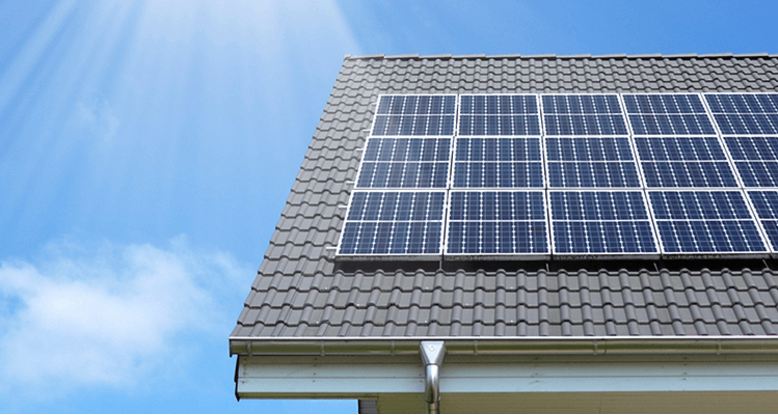
Selecting Best Mono Silicon Panels | Top 5 Features to Check
Purchase decisions should lock in modules with a conversion efficiency exceeding 22%, check for temperature coefficients lower than -0.3%/°C to withstand high heat, and confirm a 0 to +5W positive tolerance to ensure long-term high energy output.
Module Efficiency
As of 2024, market benchmark data for monocrystalline panels is as follows: mainstream P-type PERC panel efficiency ranges from 20.5% to 21.3%, while advanced N-type (TOPCon/HJT) technologies typically reach 22% to 23.2%.
When reviewing the datasheet, ensure you are looking at STC (Standard Test Conditions) values (1,000 W/m² irradiance, 25°C cell temperature).
For every 1% increase in efficiency, the power of a standard-sized panel (approximately 2 square meters) increases by about 20 W.
Efficiency and Area Conversion
Under the standard radiation intensity of 1,000 W/m², every square meter receives 1,000 watts of solar power.
If the technical specification sheet of a monocrystalline silicon module states an efficiency of 20%, this means the module can output 200 Watts of electricity per square meter;
If efficiency increases to 23%, the power output per unit area increases to 230 Watts.
This 30-watt difference per square meter is significantly amplified in common residential roof installation scenarios.
Taking a typical American single-family home roof as an example, assume the effective south-facing area available for solar panels is 40 square meters.
After excluding necessary fire lanes and obstructions like chimneys and vents, the energy output of this limited area depends entirely on module efficiency.
Using 20% efficiency modules, the total installed capacity for this area is 8 kW; whereas using 23% efficiency high-end modules (such as HJT or IBC technology), the installed capacity for the same area can reach 9.2 kW.
This additional 1.2 kW system capacity, in a region with an annual average of 4.5 sun hours per day, can generate approximately 1,971 extra kWh of electricity per year, enough to cover a significant portion of the annual charging needs for a high-efficiency heat pump or an electric vehicle.
One must be wary of the non-linear relationship between "Power" and "Efficiency" in specification sheets. There are many high-power modules on the market rated at 550W or even 600W, but this does not equate to high efficiency. Many high-power modules achieve high wattage simply by increasing physical dimensions—for example, using 210 mm wafers and increasing the number of cells, stretching the module length to 2.2 meters or even 2.4 meters. While these 20% efficiency "giant modules" might be suitable for commercial flat roofs, their excessive physical size restricts layout flexibility on residential roofs with fragmented space. In contrast, a standard-sized module measuring 1.72m x 1.13m (approx. 1.95m²), if boosted to 22.5% efficiency via TOPCon technology, can reach 440W per panel. On the same 10-meter-wide roof, standard-sized high-efficiency modules might fit perfectly in two rows, whereas giant low-efficiency modules might be forced to reduce installation by a full row because they extend 10 centimeters beyond the roof edge, leading to a significant drop in total system capacity.
When a fixed target capacity of 10 kW is required on a roof, efficiency differences directly dictate the quantity of hardware needed.
Using older PERC modules with a nominal power of 370 W (approx. 20.3% efficiency), the system requires 27 panels, covering a total area of about 51 square meters, and requiring 54 mounting points, 27 microinverters or optimizers, and longer DC cable paths.
If switching to N-type modules with a nominal power of 440W (approx. 22.8% efficiency), only 23 panels are needed to reach the same 10 kW capacity, reducing the coverage area to 43 square meters.
The reduction of four modules directly saves 15% on mounting rails, wiring terminals, and installation labor hours, while also reducing the number of roof penetrations, thereby lowering potential leak risks.
In regions with high labor costs, this hard saving on installation materials and labor driven by efficiency often offsets the premium of the high-efficiency modules themselves.
Cell spacing and packaging technology have a massive impact on the final area-to-efficiency conversion.
Traditional cell connection methods require a gap of about 2 millimeters between cells for ribbon connections. This "dead zone" does not participate in power generation but occupies module area, thereby dragging down Module Efficiency.
Modern high-density packaging technologies—such as Shingled or small-gap technology—compress cell spacing to 0.5 millimeters or even negative spacing (overlap), greatly increasing the proportion of effective power generation area.
When calculating actual roof utilization, besides looking at STC efficiency, one must also pay attention to the frame width of the module.
Although standard 30mm or 35mm aluminum alloy frames provide mechanical strength, they also constitute non-generating areas.
Some high-end Full Black modules that pursue ultimate area efficiency use optimized frame designs and busbar hiding technologies, making the actual photoelectric conversion capability per square meter approach the theoretical limit of the cells.
For complex-shaped roofs (such as multi-faceted hip roofs or roofs obstructed by skylights), high-efficiency modules allow installers to maintain a high total installed capacity while avoiding shaded areas, an "obstacle avoidance capability" that low-efficiency large-format modules lack.
Distinguishing Between Cell and Module
Currently, mainstream N-type TOPCon cells on the production line have reached an average efficiency of 25.5% or even 26.0%, but this does not mean the finished panels installed on the roof can reach the same level.
The denominator for calculating module efficiency is the entire physical contour area of the panel (including the frame, glass, and backsheet), not just the area of the silicon wafers.
When 108 or 144 cells are encapsulated into a standard module frame 1722 mm long and 1,134 mm wide, a gap of about 2 mm must be reserved between cells to buffer stress caused by thermal expansion and contraction.
Additionally, an insulation distance must be maintained between the edge of the cell string and the aluminum alloy frame. These non-generating "dead zones" directly dilute the overall energy density.
Therefore, a panel equipped with 25.5% high-efficiency cells usually only achieves a module efficiency of 22.5% to 23.0%. The 2.5% to 3.0% absolute drop in the middle is a physical inevitability caused by insufficient geometric fill factors.
Beyond geometric space waste, optical and electrical losses further widen the gap between the two.
Although photovoltaic glass is treated for high light transmission and coated with an anti-reflective coating (AR Coating), it still blocks about 3% to 4% of incident light.
The attenuation of light transmittance in EVA or POE encapsulants under long-term UV exposure is also a variable that cannot be ignored.
Deeper losses come from electrical connections: to connect hundreds of cells in series to export current, meters of metal busbars and interconnect ribbons are used inside the module.
When current travels through these metal conductors, I²R heat loss (Joule heating) occurs, and the busbars themselves shade part of the cell's light-receiving surface.
Although Multi-Busbar (MBB) and Super Multi-Busbar (SMBB) technologies reduce shading and shorten current transmission paths by thinning the ribbons, resistance losses cannot be completely eliminated.
Full black modules use black backsheets and black frames for esthetics, but this causes the gaps between cells to absorb light rather than reflect it back to the cell surface like white backsheets do.
Consequently, the efficiency of Full Black modules with the same cell configuration is often 0.1% to 0.3% lower than that of conventional modules.
Technical Parameter Comparison | Raw Cell | Finished Module | Main Physical Factors Causing Difference |
P-Type PERC | 23.0% - 23.5% | 20.8% - 21.5% | Ribbon resistance, cell gaps, glass reflection |
N-Type TOPCon | 25.0% - 26.2% | 22.0% - 23.0% | Requires better encapsulant films for water resistance, edge insulation zones |
N-Type HJT | 25.5% - 26.8% | 22.5% - 23.8% | Low-temp process demands high encapsulation standards, no busbar tech differences |
Back Contact (IBC) | 26.0% - 27.5% | 23.0% - 24.2% | No front shading, but area loss still exists at module edges |
Different packaging technologies vary hugely in their ability to control CTM (Cell-to-Module) loss, which directly determines the actual wattage the user ultimately buys.
Traditional Half-Cut packaging technology reduces internal resistance loss by splitting the cell in two to halve the current, allowing module efficiency to get closer to cell efficiency.
Shingled Technology takes a more aggressive approach, overlapping cell edges like roof tiles, completely eliminating gaps between cells, and using conductive adhesive instead of metal ribbons.
This solution maximizes the module's effective power generation area, bringing module efficiency extremely close to cell efficiency, limited only by frame and glass losses.
Another high-end solution is IBC (Interdigitated Back Contact) technology. Since both positive and negative electrodes are located on the back of the cell, there is no metal shading on the front.
Combined with high-density gapless packaging, its CTM loss rate is the lowest among all technologies.
Temperature Coefficient
The temperature coefficient (Pmax) quantifies the rate at which the power of a photovoltaic module drops when the temperature exceeds the standard test environment (25°C).
Ordinary P-type PERC monocrystalline panels usually have a coefficient between -0.34%/°C and -0.38%/°C, while advanced N-type TOPCon or HJT panels can reach -0.29%/°C or better.
When roof module temperatures reach 65°C in summer (40°C above standard), a -0.29%/°C panel retains 3.6% more of its rated power than a -0.38%/°C panel.
For a 10 kW system located in hot regions like Arizona or Australia, this parameter difference directly impacts about 550 kWh of electricity output annually.
Power Loss
According to semiconductor physics, as temperature rises, the bandgap energy of the silicon material decreases slightly, making it easier for electrons to jump.
Although this causes a negligible rise in short-circuit current (Isc) (about 0.05% per degree Celsius), the open-circuit voltage (Voc) and maximum power point voltage (Vmp) show a significant linear downward trend.
Since electrical power equals voltage multiplied by current, the substantial decay in voltage directly drags down the final power output.
This physical phenomenon occurs continuously during every sunlit period and is irreversible.
The 25°C cell temperature set by Standard Test Conditions (STC) is extremely difficult to maintain in real outdoor environments.
Solar radiation contains not only visible light but also a large amount of infrared radiation, which is absorbed by the module's glass, backsheet, and aluminum frame and converted into thermal energy.
Under passive cooling conditions without active cooling systems, the cell temperature of a module is usually 25 to 35 degrees Celsius higher than the ambient air temperature.
For example, in the summer in Nevada or Queensland, Australia, when the ambient temperature reaches 40°C, the actual operating temperature of rooftop PV modules often fluctuates between 70°C and 75°C.
This huge temperature difference makes the temperature coefficient a primary parameter to consider when calculating actual power generation, rather than just a reference indicator.
Assume a P-type PERC monocrystalline module with a nominal power of 450 Watts has a temperature coefficient of negative 0.35% per degree Celsius. When the cell temperature rises to 70°C, the temperature rise relative to standard test conditions is as high as 45°C. At this point, the power loss calculation is 45 multiplied by 0.35%, resulting in an instantaneous power loss ratio of 15.75%.
In contrast, N-type modules using Heterojunction (HJT) technology have better thermal stability due to their amorphous silicon thin-film layer structure, with a temperature coefficient typically maintained around negative 0.25% per degree Celsius.
Under the same 70°C operating condition, the power loss caused by the temperature rise is only 45 multiplied by 0.25%, which is 11.25%.
At this time, the actual output of the 450-watt module is 399 Watts. Comparing the two, the actual output difference of a single module at high temperatures reaches 20 Watts.
Over a complete life cycle, this difference accumulates into a massive power generation gap in regions with long summers and high irradiance.
The voltage drop caused by temperature also has a knock-on effect on the Maximum Power Point Tracking (MPPT) of PV inverters.
String inverters are usually set with a specific operating voltage range, such as 180 Volts to 850 Volts.
During system design, installers typically calculate the number of modules per string based on voltage under standard conditions.
However, in extreme high-temperature weather, if modules with poor temperature coefficients are selected, the total voltage of the entire string may drop significantly.
When the voltage drops close to or below the lower limit of the inverter's MPPT range, the inverter will experience a "clipping" effect, failing to track the optimal power point, or even triggering low-voltage protection to stop working in some extreme cases.
Low temperature coefficient modules can ensure high voltage levels are maintained at high temperatures, allowing for more flexible string configurations and ensuring the inverter always operates in a high-efficiency zone.
Different installation methods also amplify or reduce the degree of power loss.
Ground-mounted power stations or tilted roof systems using racking allow air circulation on the back of the modules, facilitating natural convection cooling.
For Building Integrated Photovoltaics (BIPV) or Flush Mount installations directly fitted to the roof surface, the air layer between the back of the module and the roof material is almost stagnant, making it difficult for heat to dissipate, causing the working temperature of the cells to be more than 10°C higher than that of open installations.
In such scenarios with limited heat dissipation conditions, choosing N-type TOPCon or HJT modules with low temperature coefficients becomes particularly necessary, because any additional temperature rise will be amplified into more power loss by a poorer coefficient.
Actual monitoring data shows that in regions with high average annual temperatures, the full-year "Performance Ratio" of modules with a temperature coefficient of negative 0.30% is typically 2% to 3% higher than that of modules with negative 0.38%. For owners who have signed Power Purchase Agreements (PPAs) or rely on Net Metering rates, this 2% performance ratio difference directly corresponds to a shortening or lengthening of the investment payback period.
In addition to instantaneous power output, long-term high-temperature operation also accelerates material aging.
Although the temperature coefficient itself describes reversible physical changes, when modules are under high temperature and high pressure for a long time, the risk of yellowing of encapsulation materials (EVA or POE), cracking of backsheets, and fatigue of ribbons increases.
Cell technologies with lower heat generation or better heat resistance are usually accompanied by superior encapsulation processes, which to some extent provide an implicit reliability guarantee.
When evaluating module power output, this "thermal derating" must be viewed as the norm rather than an exception, especially against the backdrop of global warming leading to frequent extreme high-temperature weather.
A module's performance above 60°C has more practical guiding significance than its parameters in a 25°C laboratory environment.
Comparison of Different Technologies
The most fundamental physical difference lies in the doping type of the substrate silicon wafer and the passivation method of the cell surface, which directly determine the recombination rate of electrons at high temperatures and thus affect the stability of the open-circuit voltage.
The market is currently in a transition phase from P-type to N-type technology.
This technological iteration is essentially to solve the performance bottlenecks of traditional cells under high temperature and low light.
Traditional P-type PERC (Passivated Emitter and Rear Contact) technology has dominated the market for the past few years.
This technology uses boron-doped silicon wafers as the substrate and employs an aluminum oxide passivation layer on the back.
Although PERC has made great strides compared to earlier Aluminum Back Surface Field (BSF) technology, limited by the material properties of P-type silicon wafers, the recombination rate of holes and electrons remains high at elevated temperatures.
The temperature coefficient of standard P-type PERC modules usually hovers between negative 0.34% and negative 0.39% per degree Celsius.
When the cell temperature rises, the thermal motion of carriers inside the silicon material intensifies, leading to increased leakage current and a significant voltage drop.
On a typical 400-watt PERC module, if the operating temperature reaches 65°C, the power attenuation magnitude will usually exceed 15%, and the actual output power will drop directly below 340 Watts.
To break through this physical limit, the industry has begun a large-scale shift to N-type TOPCon (Tunnel Oxide Passivated Contact) technology.
TOPCon uses phosphorus-doped N-type silicon wafers.
This material itself has a higher tolerance for metal impurities and does not suffer from Light Induced Degradation (LID) caused by boron-oxygen complexes.
TOPCon introduces an ultra-thin silicon oxide tunnel layer and a doped polysilicon layer on the back of the cell.
This structure allows electrons to pass through smoothly while blocking holes, greatly reducing the recombination rate in the metal contact area.
Due to the significant improvement in surface passivation, the open-circuit voltage (Voc) of TOPCon modules can be made higher, typically reaching 710 mV to 720 mV, and high voltage is a natural barrier against high-temperature attenuation.
This allows TOPCon's temperature coefficient to be optimized to negative 0.29% to negative 0.32% per degree Celsius.
In the same high-temperature environment, TOPCon modules can retain about 2% to 3% more power generation capacity than PERC modules.
At the top of the pyramid in terms of heat resistance is HJT (Heterojunction) technology.
HJT adopts a completely different "sandwich" structure, depositing intrinsic amorphous silicon thin films and doped amorphous silicon thin films on both the front and back sides of an N-type monocrystalline silicon wafer.
The amorphous silicon layer has an extremely wide bandgap, which can perfectly passivate the dangling bonds on the surface of the crystalline silicon, almost completely eliminating surface recombination losses.
This superior passivation effect enables the open-circuit voltage of HJT cells to break through 750 mV.
Physics laws indicate that the higher the open-circuit voltage of a cell, the lower the absolute value of its temperature coefficient.
Therefore, the temperature coefficient of HJT modules can reach an astonishing negative 0.25% to negative 0.27% per degree Celsius.
In hot desert or equatorial regions, the power generation advantage of HJT increases linearly with the rise in temperature. This technical characteristic makes it the preferred solution for high-temperature conditions, despite its complex manufacturing process and relatively higher cost.
Another high-end technology is IBC (Interdigitated Back Contact) and its derivatives (such as the technology used by Maxeon).
All electrodes of IBC are located on the back of the cell, with no grid line shading on the front, maximizing the light-receiving area.
Although IBC is mainly known for high conversion efficiency, its N-type substrate and excellent back contact design also endow it with excellent temperature characteristics.
Quality IBC modules typically have a temperature coefficient around negative 0.29% per degree Celsius, and some IBC products combined with passivation contact technology can even approach the level of HJT.
Unlike HJT, which relies on amorphous silicon layers, IBC maintains high voltage through extreme structural design.
The table below details the actual power performance comparison of different technology routes under an ambient temperature of 35°C (leading to a module temperature of approx. 65°C).
Assume the nominal power (STC) of all modules is 450 Watts to quantify the real production capacity gap caused by the technological generation difference.
Technology Type | Wafer Polarity | Typical Temp Coefficient | 65°C Temp Rise Loss (ΔT=40°C) | Actual Output at 65°C | Power Gain vs PERC |
P-type PERC | P-Type (Boron doped) | -0.38% / °C | 15.2% | 381.6 W | - |
P-type PERC (Optimized) | P-Type (Boron doped) | -0.35% / °C | 14.0% | 387.0 W | +5.4 W |
N-type TOPCon | N-Type (Phosphorus doped) | -0.30% / °C | 12.0% | 396.0 W | + 14.4 W |
N-type IBC | N-Type (Phosphorus doped) | -0.29% / °C | 11.6% | 397.8 W | + 16.2 W |
N-type HJT | N-Type (Phosphorus doped) | -0.26% / °C | 10.4% | 403.2 W | + 21.6 W |
From the data, it is intuitively visible that although the nominal power is 450 Watts for all, in actual high-temperature operation, the HJT module outputs 21.6 Watts more instantaneous power than the standard PERC module.
For a 10 kW residential PV system (approx. 22 panels), choosing HJT technology over traditional PERC technology yields about 475 Watts more power output at noon in summer.
This 475-Watt difference does not stem from changes in light intensity, but is purely determined by the reaction of the cell's physical structure to heat.
In the long run, this performance gain brought by technology selection can effectively offset the higher initial procurement cost of N-type modules, especially in regions with expensive electricity or favorable net metering policies, where the payback period for the technology premium will be significantly shortened.
Cell Technology
Compared to the 22.8% theoretical efficiency ceiling of P-type PERC modules, the mass production efficiency of N-type TOPCon and HJT has generally exceeded 25%.
N-type cells do not suffer from initial Light Induced Degradation (LID) caused by boron-oxygen recombination; first-year degradation can be controlled within 1%, and linear degradation is as low as 0.4% per year.
Over a 25-year lifecycle, the total power generation of N-type modules is typically 3% to 5% higher than that of P-type, making it the best current solution for balancing cost and output.
Difference Between P-type and N-type
For the P-type silicon wafers that have dominated the market for the past decade, manufacturers doped the crystal lattice with Boron to form positive charge holes.
When the module is first exposed to sunlight after installation, boron atoms rapidly react chemically with permeating oxygen atoms to form Boron-Oxygen complexes.
These complexes capture electrons, causing the module power to permanently drop by 2% to 3% within the first few weeks of operation.
This is what the industry knows as Light Induced Degradation (LID).
Although current P-type PERC modules can mitigate this issue by doping with Gallium, the process difficulty of controlling resistivity uniformity is extremely high due to the low distribution coefficient of Gallium in silicon, and it cannot completely eliminate the influence of boron-oxygen pairs from the physical root.
In contrast, N-type silicon wafers use Phosphorus as the dopant.
There is no similar recombination trap formation between phosphorus atoms and oxygen atoms, cutting off the LID generation path from the underlying material logic.
In third-party laboratory test data, the initial light degradation of N-type modules is often undetectable or remains steadily within the measurement error range of 0.5% to 1%.
For a 100 MW utility-scale power station project, just reducing the first-year degradation rate from 2.5% to 0.5% is equivalent to directly recovering 2 MW of installed capacity loss in the early stage of the project.
Minority Carrier Lifetime is the most basic physical parameter measuring a cell's ability to convert photons into current. Under standard resistivity, the minority carrier lifetime of P-type monocrystalline silicon wafers is usually limited to between 80 microseconds and 200 microseconds.
N-type monocrystalline silicon wafers have a higher tolerance for common metal impurities (such as interstitial iron), and their minority carrier lifetime is usually an order of magnitude higher than that of P-type, easily reaching over 1,000 microseconds (1 millisecond).
The prolonged survival time of electrons in N-type silicon wafers directly increases the cell's Open Circuit Voltage (Voc) and Short Circuit Current (Isc).
This is why the mass production efficiency of TOPCon cells based on N-type wafers can quickly break through 25%, while P-type PERC cells, even after several passivation process improvements, remain stuck at the theoretical ceiling of 23.5%, unable to advance.
This material-level performance gap becomes more pronounced as cells become thinner, because N-type wafers can maintain extremely high photoelectric conversion integrity even at thinner thicknesses.
The difference in temperature coefficients stems from the different behaviors of the Fermi level of the silicon-based material with temperature changes.
The power temperature coefficient of standard P-type modules is typically -0.34% / °C to -0.38% / °C.
When the ambient temperature reaches 40°C, the module surface temperature often rises to 65°C or even higher.
Under these conditions, the power of P-type modules will lose 13.6% to 15.2%.
The temperature coefficient of N-type TOPCon modules is usually optimized to -0.29% / °C, and the power loss under the same high temperature is about 11.6%.
For HJT (Heterojunction) technology, this figure is as low as -0.26% / °C.
In equatorial regions or geographical latitudes with long summers, this difference in performance retention at high temperatures leads to the actual annual power generation of N-type modules being about 3% higher than P-type modules of the same nominal power.
Bifaciality refers to the ratio of rear-side efficiency to front-side efficiency.
In bifacial generation modules, P-type PERC cells typically have a bifaciality of only 70% ± 5% due to the limitations of the aluminum back surface field design which shades more light.
If the front side is 400W, the back side can only contribute efficiency equivalent to 280W under ideal light reception.
N-type cells (especially TOPCon and HJT) naturally feature symmetrical structural designs; the rear electrode grid lines can be made as thin and narrow as the front, eliminating rear shading area.
The bifaciality of N-type modules can generally reach 80% (TOPCon) or even 85% (HJT).
In high-reflectivity scenarios like cement floors or white roofs (Albedo > 50%), just a 10% increase in bifaciality can add an extra 2% to 3% to the overall system power generation gain.
TOPCon Technology
The essential physical breakthrough of TOPCon (Tunnel Oxide Passivated Contact) technology lies in its successful preparation of an ultra-thin silicon dioxide layer on the back of the cell, with thickness precisely controlled between 1.5 nanometers and 2 nanometers.
This oxide layer is thin enough to utilize the quantum tunneling effect, allowing electrons to pass through unimpeded like "walking through a wall," while strictly blocking the transport of holes using the potential barrier height difference.
Closely adhering to this oxide layer is a highly doped polysilicon layer; together they form the passivation contact structure.
This structure physically isolates the metal electrode from the crystalline silicon substrate, fundamentally eliminating the high recombination rate area that occurs when metal contacts silicon directly.
In traditional PERC cells, the metal contact area on the back is the main "leakage point" for minority carrier recombination, limiting the increase of open-circuit voltage.
TOPCon cells, relying on this passivation contact mechanism, can suppress the rear recombination current density (J0) from 40 fA/cm² in the PERC era to below 10 fA/cm², directly pushing the cell's open-circuit voltage (Voc) from 685 mV to the 710 mV to 720 mV range.
For users, higher open-circuit voltage directly corresponds to better low-light startup voltage, allowing the inverter to start working about 15 to 30 minutes earlier in the morning compared to PERC systems.
The broadening of the spectral response range is another substantive gain brought by TOPCon.
Standard crystalline silicon cells respond well to short-wavelength light (blue light/UV), but tend to suffer from quantum efficiency drops in the long-wavelength region (red light/infrared).
TOPCon's rear passivation structure significantly improves the absorption and utilization rate of near-infrared light in the 800 nm to 1100 nm band.
During sunrise and sunset periods as well as cloudy weather, the proportion of infrared light in the solar spectrum increases; TOPCon cells can capture this light energy and convert it into current.
Field test data shows that under the same nominal power, relying solely on superior long-wave response, the power generation per watt of TOPCon modules under low irradiance conditions (200 W/m² - 400W/m²) is 2% to 3% higher than PERC.
This all-weather cumulative effect makes the actual power generation advantage of TOPCon more obvious in Nordic or foggy regions with lower annual average irradiance than in strong-light desert regions.
In the game between manufacturing processes and material costs, the consumption of silver paste by N-type silicon wafers used in TOPCon was once an obstacle to its commercialization.
Early TOPCon cells required silver paste on both sides, and to penetrate the front silicon nitride anti-reflective coating and form good contact, the silver consumption per cell reached 150 mg to 160 mg, far higher than the 90 mg level of PERC.
With the introduction of SMBB (Super Multi-Busbar) and 0BB (No Busbar) technologies, silver paste usage is declining rapidly.
More worthy of attention is the matching of encapsulation materials. The silver-aluminum paste on the front of N-type TOPCon cells is more sensitive to water vapor and prone to electrochemical corrosion.
Therefore, many top-tier manufacturers have abandoned traditional EVA (Ethylene-Vinyl Acetate) films in TOPCon modules, switching to POE (Polyolefin) films or EPE co-extruded films which have water resistance two orders of magnitude higher.
POE films not only block water vapor but also completely eliminate the risk of acetic acid produced by EVA decomposition corroding cell grid lines. They also possess higher volume resistivity, excellently suppressing PID (Potential Induced Degradation) phenomena.
When users check the BOM (Bill of Materials), confirming that the encapsulation film type is POE or EPE is an important basis for judging whether the TOPCon module possesses 30-year weather resistance.
Performance Indicator | P-type PERC (Mainstream) | N-type TOPCon (Advanced) | Practical Application Difference |
Theoretical Limit Efficiency | 24.50% | 28.70% | TOPCon still has significant room for process upgrades, unlikely to be obsolete soon. |
Mass Production Cell Voc | < 690 mV | > 710 mV | High voltage brings better inverter matching efficiency and earlier startup times. |
Bifaciality | 70% ± 5% | 80% ± 5% | On cement or light-colored roofs, TOPCon rear generation gain is over 10% higher. |
Power Temperature Coefficient | -0.34% / °C | -0.29% / °C | At 60°C working temp, TOPCon power retention is about 1.75% higher. |
Low Light Response (Long Wave) | Average | Excellent | On cloudy days or mornings/evenings, TOPCon power output curve is fuller. |
PID Sensitivity | Medium | Very Low (Requires POE) | N-type substrate is naturally immune to positive high voltage PID, longer life with POE. |
From the perspective of mass production equipment, TOPCon production lines have a compatibility of up to 60% to 70% with existing PERC lines.
Manufacturers only need to add core equipment such as boron diffusion, LPCVD (Low Pressure Chemical Vapor Deposition) oxidation, and coating to existing lines to complete the upgrade.
This lower capital expenditure (CapEx) threshold allows global photovoltaic capacity to shift to TOPCon on a large scale in a short time, rapidly diluting R&D and depreciation costs.
Currently, the price difference between TOPCon modules and PERC modules on the market has compressed to within $0.01/Watt.
Considering its warranty commitment of only 1% first-year degradation (PERC is 2%) and 0.4% annual linear degradation (PERC is 0.55%), at the end of a 25-year lifecycle, the power output retained by TOPCon modules will be 4% to 5% higher than PERC.
Even without calculating bifacial generation and high-temperature gains, the extra power generation over the full lifecycle brought solely by the degradation rate advantage is enough to cover its tiny initial premium.
For residential users seeking to maximize power generation per unit area due to limited roof space, or ground power stations sensitive to land rent, using 72-cell version TOPCon modules with 182mm or 210mm wafers, the power per panel has generally reached 570W to 580W, 20W to 30W higher than PERC modules of the same size, significantly reducing the per-watt Balance of System (BOS) costs for racking, cabling, and installation labor.
HJT Heterojunction
Heterojunction (HJT) cells completely overturn the single-material concept of traditional crystalline silicon cells in physical structure, adopting a stacking process similar to a "sandwich."
Its core is the deposition of extremely thin intrinsic amorphous silicon passivation layers and doped amorphous silicon layers on both the front and back sides of an N-type monocrystalline silicon wafer.
The thickness of these two amorphous silicon films is only 5 nanometers to 10 nanometers, yet they perfectly repair dangling bond defects on the crystalline silicon surface at the atomic level.
Because amorphous silicon has a high hydrogen content, hydrogen atoms can deeply passivate defect states at the silicon wafer interface, allowing the open-circuit voltage (Voc) of HJT cells to easily break through 740 mV, even approaching the theoretical limit of 750 mV.
In comparison, the open-circuit voltage of mainstream TOPCon cells is usually between 710 mV and 720 mV.
This extremely high open-circuit voltage not only represents higher photoelectric conversion efficiency potential but also endows the module with excellent resistance to Potential Induced Degradation (PID), because the amorphous silicon layer naturally blocks leakage current paths, and the conductivity of the surface Transparent Conductive Oxide (TCO) film completely eliminates surface polarization phenomena.
Since the lateral conductivity of the amorphous silicon layer is extremely poor, HJT cells must rely on the Transparent Conductive Oxide (TCO) film deposited on the outermost layer to collect and transmit current.
This thin film, usually composed of Indium Tin Oxide (ITO), combines light transmission and conductivity. The introduction of the TCO process replaces the PN junction formation via traditional high-temperature diffusion processes, meaning the entire manufacturing process of HJT completely avoids high-temperature environments.
The sintering step for traditional PERC or TOPCon cells reaches temperatures as high as 750°C to 850°C, while the full process temperature of HJT is strictly controlled within 200°C.
This low-temperature process greatly reduces thermal stress and warping risks inside the silicon wafer, making HJT the best carrier for the wafer thinning trend.
Currently, the standard wafer thickness in the industry is 130 microns to 150 microns, while HJT production lines can already batch process ultra-thin wafers with a thickness of only 100 microns or even 90 microns without increasing breakage rates.
Silicon accounts for the highest proportion of total cell cost; every 10-micron reduction can lower silicon costs by about 3% to 4%. This thinning capability is an important moat for HJT to counter silver paste cost disadvantages in the future.
· Temperature Coefficient Advantage:
The most lethal characteristic of HJT lies in its extremely low temperature coefficient, usually between -0.24% / °C and -0.26% / °C. The output power of crystalline silicon cells drops as temperature rises, mainly caused by voltage drop. Since HJT possesses an extremely high open-circuit voltage base, and the band structure of amorphous silicon material changes little with temperature, its voltage decay with rising temperature is far smaller than that of conventional crystalline silicon. At noon in summer, when the module surface temperature rises to 65°C (40°C higher than STC standard), PERC modules (-0.34%/°C) lose about 13.6% power, while HJT modules lose only about 10%. In hot Middle Eastern or Australian desert regions, measured data shows HJT modules generate 4% to 6% more power per watt annually than PERC, and 1.5% to 2% more than TOPCon.
· Bifaciality:
Complete structural symmetry endows HJT with naturally high bifaciality. PERC module rear is shaded by aluminum grid lines and back fields, with bifaciality only around 70%; TOPCon can reach 80% after optimization; while HJT cell front and rear structures are basically identical, with bifaciality generally reaching 85% or even higher. In high-reflection scenarios like snow, white roofs, or light-colored cement (reflectivity > 60%), this extra 5% to 15% rear gain can significantly boost total system power generation.
· Micro-crystalline Technology Upgrade:
Early HJT used pure amorphous silicon layers, which had issues with parasitic light absorption loss and low Fill Factor (FF). The latest mass production technology has introduced Microcrystalline Silicon to replace the doped amorphous silicon layer. Microcrystalline silicon has higher doping efficiency and lower contact resistance, significantly improving carrier mobility. After introducing the micro-crystalline process, the short-circuit current density (Jsc) of HJT cells increased, and the Fill Factor rose from 82% to over 84%, directly driving cell mass production efficiency up by about 0.5%.
Due to the necessity of curing below 200°C, standard high-temperature sintered silver paste cannot be used; instead, low-temperature silver paste, which is more expensive and has slightly weaker conductivity, must be used.
Although HJT silver consumption has been reduced from the early 200 mg/cell to around 100 mg/cell through 0BB (No Busbar) technology and the application of silver-coated copper paste, a cost premium still exists compared to TOPCon.
Additionally, Indium used in TCO coating is a rare metal, and fluctuations in Indium prices directly affect HJT's non-silicon costs.
Current solutions include developing low-indium or indium-free TCO stacks (such as using AZO aluminum-doped zinc oxide to replace part of the ITO), which have been able to reduce indium usage by 50%, gradually leveling the cost gap with TOPCon.
For investors pursuing an ultra-long lifecycle of over 25 years, HJT modules' extremely low degradation rate (1% first year, 0.35% linear) ensures they still maintain over 88% power output in the 30th year.
Warranty Terms
Monocrystalline silicon panel warranties are actually divided into two parts: a 12 to 25-year Product Workmanship Warranty (against manufacturing defects) and a 25 to 30-year Linear Performance Warranty.
For mainstream monocrystalline PERC modules, the industry standard is no more than 2% degradation in the first year, and less than 0.55% annually thereafter, ensuring output power is above 84.8% in the 25th year.
In contrast, high-quality N-type modules (like REC or Maxeon) typically provide a double 25-year guarantee, with power retention around 92% in the 25th year.
Workmanship Warranty Duration
For most top-tier monocrystalline silicon module manufacturers, the standard product workmanship warranty period is set at 10 to 12 years.
This time point is not chosen arbitrarily but is based on statistical results from physical aging curves of polymer backsheets and ethylene-vinyl acetate (EVA) encapsulation films under outdoor UV and thermal cycling.
In actual operation, the risk of standard modules developing backsheet yellowing, cracking, and seal failure leading to moisture intrusion rises significantly after the 12th year. Once moisture enters the module, it rapidly triggers circuit corrosion and PID (Potential Induced Degradation) effects.
In comparison, brands at the top of the market like Maxeon (spun off from SunPower), REC Solar's Alpha series, or Silfab's Elite series directly extend the workmanship warranty to 25 years, with some models even reaching 40 years, by changing the Bill of Materials (BOM).
This difference in warranty duration, which is more than double, mainly stems from fundamental differences in physical structure, such as using Glass-Glass encapsulation to replace the traditional glass-backsheet structure, or using N-type cell connection technology with higher UV resistance, thereby eliminating backsheet aging as the most common failure point.
"In North American and European markets, the cost of a standard truck roll for service is typically between $150 and $300, not including the electrician's labor fee of $75 to $120 per hour. If your module only has a 10-year material warranty and a junction box failure occurs in the 13th year, even if the market salvage value of the panel itself is only $100, the total cost you pay to fix the fault will far exceed the cost of buying a new panel."
Standard warranty terms usually cover bypass diode failure within the junction box, which is the main physical cause of local hot spots and significant string power drops.
High-quality warranty terms require the junction box protection rating to reach IP68 and guarantee that the sealing ring will not embrittle or fail under extreme temperature differences from -40°C to +85°C.
Regarding connectors, although most panels come factory-equipped with original Stäubli MC4 connectors, some low-cost manufacturers may mix in "MC4 compatible" third-party connectors. The arc risk and burnout caused by mismatched contact resistance must be explicitly included in the workmanship warranty scope.
If you are purchasing AC Modules integrated with microinverters (e.g., Enphase IQ series) (such as Maxeon 6 AC or Qcells Q. TRON BLK G2+), you need to confirm whether the workmanship warranty covers both the panel and the microinverter.
Typically, the warranty period for such integrated products is unified to 25 years, avoiding finger-pointing over failure responsibility between panel and inverter manufacturers.
In terms of mechanical strength, the workmanship warranty is also directly related to the panel's ability to withstand snow and wind loads.
Standard warranties are usually based on the IEC 61,215 standard, covering 5400 Pa (Pascal) snow load on the front and 2400 Pa wind load on the back.
However, users in high-latitude snowy regions or coastal hurricane zones need to pay attention: some reinforced modules (like the REC TwinPeak series) increase capacity to over 7000 Pa by adding strengthening ribs on the back of the frame.
Their warranty terms will explicitly state that frame deformation occurring in high-load environments is covered, whereas ordinary modules crushed by heavy snow exceeding 5400 Pa are usually denied compensation by manufacturers on grounds of "force majeure" or "exceeding design load."
Furthermore, for systems installed in salt mist environments (coastal) or high ammonia environments (farms), one must check if the warranty terms include IEC 61701 (Salt Mist Corrosion) and IEC 62716 (Ammonia Corrosion) compliance statements; otherwise, metal part corrosion and performance degradation appearing in these specific environments will not be covered.
Linear Power Output
Under old terms, if a panel's efficiency dropped to 91% in the 9th year but suddenly fell to 82% in the 10th year, the manufacturer bore no responsibility because this was still above the "80%" step.
Current linear warranties force manufacturers to be responsible for power loss every single year by locking in the maximum allowable degradation value per year.
For standard P-type monocrystalline PERC panels, the widely accepted industry baseline is: first-year degradation not exceeding 2.0% or 2.5%, and linear degradation thereafter not exceeding 0.55% annually.
Based on this mathematical model, a panel nominally rated at 400 W will retain about 84.8% of its initial value after 25 years of operation.
This 84.8% is the passing line in the current monocrystalline silicon market; any warranty commitment lower than this figure indicates that the module uses lower-grade encapsulation materials or cells.
The first-year degradation rate is the first threshold distinguishing ordinary panels from top-tier panels and is also the area with the largest data discrepancy.
Due to Boron doping during crystal pulling, P-type monocrystalline silicon forms Boron-Oxygen defects when first exposed to sunlight, capturing electrons and leading to Light Induced Degradation (LID).
This physical reaction causes the module to permanently lose 2% to 3% of power within the first few weeks of installation.
In contrast, panels using N-type technology (like TOPCon or HJT) use Phosphorus doping, fundamentally eliminating boron-oxygen complexes.
Therefore, series like Jinko Solar's Tiger Neo or REC's Alpha Pure can commit to a first-year degradation rate of 1.0% or even lower.
This 1.5% first-year gap directly translates into a 1.5% power generation base difference over the system's full lifecycle. For a 10 kW home system, this equates to thousands of kilowatt-hours wasted over 25 years.
The Annual Degradation Rate entering the second year mainly reflects the anti-aging capability of encapsulation materials.
Although 0.55% is the industry standard, high-end modules have compressed this figure to the 0.25% to 0.4% range.
The reason for this difference lies in cell surface passivation technology and the choice of encapsulation film (EVA vs POE).
Ordinary EVA film produces acetic acid under long-term UV exposure, slowly corroding cell grid lines, leading to increased series resistance and year-by-year power decline.
High-end N-type modules often use Glass-Glass encapsulation or Polyolefin Elastomer (POE) film, which has higher water resistance and does not release acidic substances, allowing annual degradation to be controlled around 0.3%.
The table below shows specific data differences in warranty terms for monocrystalline silicon panels of different technology routes:
Technology Type | Typical Representative Series | First Year Degradation Commitment | Annual Degradation Commitment (Year 2–25) | 25-Year End Power Guarantee | 30-Year End Power Guarantee |
Standard P-Type PERC | Canadian Solar HiKu6, Trina Vertex S | ≤ 2.0% | ≤ 0.55% | 84.8% | N/A (Usually only 25-year warranty) |
N-Type TOPCon | Jinko Tiger Neo, Qcells Q. TRON | ≤ 1.0% | ≤ 0.40% | 89.4% | 87.4% |
N-Type HJT | REC Alpha Pure, Huasun Himalaya | ≤ 1.0% | ≤ 0.25% | 92.0% | 90.0% |
IBC (Interdigitated Back Contact) | Maxeon 6 (SunPower) | ≤ 2.0% (Incl. measurement error) | ≤ 0.25% | 92.0% | 88.25% (40 years) |
At the end of a cycle as long as 25 or even 30 years, this tiny annual percentage difference accumulates into a massive performance chasm.
Taking the 25-year end power guarantee as an example, standard PERC modules commit to remaining 84.8% power, while top-tier HJT or IBC modules commit to remaining 92%.
This 7.2% difference is not negligible; in the system's later years, high-end panels can still maintain output capacity close to new panels, while ordinary panels may no longer meet the household's growing electricity load.
For modules adopting Bifacial technology, although warranty terms usually only make written commitments for front-side power, the physical mechanism of rear-side degradation is the same as the front.
If the front uses a double-glass structure, due to the glass's absolute barrier to water vapor, the rear power degradation of such modules is usually also superior to transparent backsheet modules.
Labor and Shipping Details
Logistics costs for transporting this 20 to 25 kg module from the warehouse to your home, old module removal costs, new module installation costs, and freight for shipping the faulty module back to the factory for failure analysis are usually fully borne by the system owner.
In North American and Western European markets where labor costs are high, this hidden expense often far exceeds the salvage value of the module itself.
PV system maintenance typically requires two licensed electricians to work on-site to meet OSHA or local safety codes (especially involving roof work).
The base truck roll fee plus labor for the first two hours for a single visit is universally between $300 and $500.
Before the manufacturer agrees to ship a replacement, they usually require the user to provide a detailed on-site test report to prove the fault was not caused by the external environment.
This requires a licensed installer to bring a professional IV Curve Tracer or thermal imager to the site, disconnect the string, and perform independent Open Circuit Voltage (Voc) and Short Circuit Current (Isc) tests on the suspected faulty panel.
This diagnostic fee is typically not covered by the standard warranty. If the test results show the panel is normal (i.e., a "false alarm"), or the cause of failure is determined to be force majeure, the user not only has to bear hours of senior electrician diagnostic fees himself but may also face "no fault found" lab testing fees charged by the manufacturer.
To avoid these risks, one must carefully review the specific definitions regarding "Labor Reimbursement" in the warranty terms. Different tiers of brands distinguish themselves significantly here:
1. Standard Material Warranty:
The standard series of the vast majority of Tier 1 brands fall into this category. Terms explicitly state they are not responsible for any on-site labor, removal, installation, or troubleshooting costs. The user receives a new panel in a cardboard box, and all remaining logistics and installation steps must be solved at their own expense.
2. Fixed Rate Reimbursement:
Some mid-to-high-end brands (like Qcells or some Jinko N-type series) set fixed labor compensation standards in their warranty terms. For example, the terms might stipulate that for every replaced panel, the manufacturer pays the installer a flat labor subsidy of $125 or $150. However, if the market rate for licensed electricians in your area is $150/hour with a 2-hour minimum, the user still needs to make up the $150 to $200 difference between the actual bill and the manufacturer's subsidy.
3. All-Inclusive / Complete Confidence Warranty:
This is the top-tier protection, typically offered by Maxeon (SunPower), Panasonic (AllGuard), or REC (ProTrust). These terms explicitly cover the full costs of diagnosis, shipping (both ways), removal, and reinstallation. If a Maxeon panel fails, after remote data verification, the manufacturer will dispatch a certified installer with a new panel to the door, and the user pays nothing.
For systems using Microinverters or Power Optimizers, the delineation of responsibility for labor costs is more complex.
If using AC Modules (panels integrated with microinverters at the factory), one must confirm if the warranty terms treat the panel and microinverter as a Single SKU.
In some split installations, if the microinverter fails, the panel manufacturer's warranty terms do not cover the labor cost of removing the panel to access the inverter underneath, while the inverter manufacturer's warranty might only cover the replacement of the inverter itself.
The integrated warranty of AC modules eliminates this "finger-pointing" risk, ensuring that whether it is an inverter or panel failure, as long as roof work is required, all relevant labor and transportation costs are borne by the warranty terms of the same parent company.
When calculating the 25-year Levelized Cost of Energy (LCOE) of a PV system, the difference in this clause is enough to alter the ROI model.
Mechanical Load & Durability Ratings
Qualified monocrystalline silicon modules must indicate static load data of 5400 Pa front (approx. 112 psf, for withstanding snow) and 2400 Pa rear (approx. 50 psf, for resisting strong wind) in the specification sheet.
In terms of durability, modules must pass the hail test in the IEC 61,215 standard, which involves withstanding a 25 mm diameter ice ball impacting at a speed of 23 meters/second without breaking.
Frame Material Thickness
Although current industry trends tend to cut frame thickness from the traditional 40mm or even 50mm to 30mm to reduce logistics and material costs, this lightweight design compromises physical performance.
The height (i.e., thickness) of the frame is directly related to the moment of inertia, which is a data point measuring the material's ability to resist bending deformation.
When the frame height is reduced from 40 mm to 30 mm, under the same 5400 Pa static load, the vertical deformation at the center of the module increases significantly.
This deformation causes the glass to bend downward, crushing the junction box below, or worse, causing the silicon wafers encapsulated in the EVA film to fracture.
For projects installed on flat roofs or requiring tilted racking, 35 mm should be considered the minimum threshold for guaranteeing structural rigidity, while 30 mm frame products are typically only suitable for flush mounts or low wind pressure zones.
Besides geometric dimensions, the alloy grade and heat treatment process of the aluminum material determine the hardness and yield strength of the metal.
Most Tier 1 manufacturers use 6063-T5 or 6063-T6 series aluminum alloys. Here, "6063" represents aluminum-magnesium-silicon alloy, which has good extrusion performance and corrosion resistance;
"T5" and "T6" represent heat treatment states. The T6 state has undergone artificial aging treatment, and its hardness and tensile strength are usually 10% to 15% higher than T5.
When consulting the technical specification sheet, if the specific alloy state is not indicated, or if lower strength 6060 alloy is used, the frame's ability to resist deformation under extreme wind loads will be greatly discounted.
When the module is subjected to 2400 Pa wind suction (negative pressure), softer aluminum is more prone to plastic deformation at the clamp positions, leading to loose clamps or even module detachment.
The anodization process forms a dense aluminum oxide protective film on the surface of the aluminum material to isolate air and moisture and prevent corrosion.
In standard IEC tests, the average thickness of the anodized layer is usually required to reach 15 microns (AA15) or more to adapt to coastal or high-humidity environments.
However, many low-cost modules control the oxide layer thickness to 10 microns (AA10) or even lower to save electrolysis costs.
In dry continental climates, AA10 is indeed usable, but if the installation environment is within five kilometers of the coastline, salt mist will rapidly penetrate the thin oxide layer, causing pitting corrosion on the aluminum material.
The connection between photovoltaic glass and the aluminum frame is not rigid but relies on RTV silicone sealant filled in the "U"-shaped groove of the frame.
The width and depth of this U-shaped groove must reserve enough space to accommodate the silicone. If the frame thickness is compressed, the U-shaped groove often becomes shallower, reducing the contact area of the silicone.
According to lab data, Peel Strength must be greater than 40 N/cm to ensure the glass does not separate from the frame during long-term thermal expansion and contraction cycles.
Excessively thin frames often fail to provide sufficient glue groove depth, making it easy for moisture to invade the module interior through the aging glue layer, leading to PID (Potential Induced Degradation) effects.
Hail Test Standards
The standard baseline test requires using an ice ball with a diameter of 25 mm and a mass of about 7.53 g, accelerated by a pneumatic launcher to a terminal velocity of 23.0 m/s, to impact the module surface vertically.
To simulate the real physical state of hail in nature, the test ice balls must be stored frozen in an environment of -4°C to -17°C and must be launched within 60 seconds of removal from the freezer container to ensure the ice ball remains a hard solid structure at the moment of impact rather than a slushy mixture.
The impact is not random; laboratory technicians will select 11 specific weak points based on the module's geometric structure for precision strikes, including corners, edges, cell centers, connection points between two cells, and the glass area directly above the junction box.
Any glass breakage or backsheet perforation at any point will be directly judged as a failure, but visible integrity is only the first step of passing the test.
The module must also maintain electrical insulation performance in the subsequent wet leakage current test, and maximum power degradation must not exceed 5%.
The kinetic energy formula in physics indicates that impact energy is proportional to mass and proportional to the square of velocity; a tiny increase in hail diameter leads to an exponential rise in destructive power.
Although the 25 mm ice ball test represents common weather conditions in most regions, generating impact kinetic energy of about 1.99 Joules, this is far from enough for users located in the US Midwest "Hail Alley" or high-risk regions in Australia.
As climate patterns change, hail exceeding 40 mm in diameter is becoming increasingly common.
When the ice ball's diameter increases to 35 mm, its mass increases to 20.7 g. At a test speed of 27.2 m/s, the impact kinetic energy surges to 7.65 Joules, nearly four times that of the standard test.
High-end module manufacturers usually refer to the ANSI FM 4,473 standard for stricter testing.
This standard divides hail resistance into four classes, where Class 4 requires the module to withstand a 50.8 mm (2-inch) ice ball impacting at 32.0 m/s, generating kinetic energy exceeding 30 Joules.
Test Class | Ice Ball Diameter (mm) | Ice Ball Mass (g) | Impact Speed (m/s) | Impact Kinetic Energy (Joules) | Destructive Power Description |
IEC 61215 (Base) | 25 | 7.53 | 23.0 | 1.99 | Equivalent to moderate intensity hail, most qualified modules pass easily. |
Enhanced Test (Tier 1) | 35 | 20.7 | 27.2 | 7.65 | Kinetic energy approx. 4x base standard, screens out products with poor glass tempering. |
FM 4473 Class 3 | 45 | 43.9 | 30.7 | 20.7 | Extremely high risk. Only modules with thickened glass or special encapsulation survive. |
FM 4473 Class 4 | 50.8 | 62.0 | 32.0 | 31.7 | Catastrophic hail. Impact force enough to penetrate some thin-film modules or shatter ordinary 3.2mm glass. |
In the Hail Stress Sequence of third-party independent laboratories like PVEL (PV Evolution Labs), after receiving hail impact, modules must undergo several thermal cycles and mechanical load tests before finally undergoing EL (Electroluminescence) imaging inspection.
This is because the high-speed impact of hail, even if it does not shatter the surface tempered glass, sends shockwaves through the EVA film to the silicon wafers inside, which are only 160 to 180 microns thick.
This impact generates micro-cracks invisible to the naked eye inside the silicon wafer. Although they do not significantly affect power output in the initial stage, during subsequent thermal expansion and contraction processes, these micro-cracks will rapidly expand, eventually leading to open circuits or severe local hot spots.
This is why, when looking at module specification sheets, one must not only check if it passed IEC 61215 but also confirm if there are internal damage reports based on EL imaging.
Glass thickness and heat treatment processes are the main variables determining impact resistance.
Currently, mainstream single-glass modules on the market typically use 3.2mm fully tempered glass.
After high-temperature heating and rapid cooling, a strong compressive stress layer forms on the surface, usually allowing it to pass 35 mm or even 45 mm impact tests relatively well.
However, with the popularization of bifacial double-glass modules, to control weight, many manufacturers have reduced glass thickness to 2.0 mm.
Although 2.0 mm glass is also heat strengthened, its surface stress is usually lower than fully tempered glass, and its physical strength is weaker.
When facing hail exceeding 30 mm in diameter, the back glass (backlight side) of 2.0 mm double-glass modules is often more prone to breakage than the light-receiving side because the back lacks direct support from the aluminum frame and the stress mode is different.
For users living in hail-prone areas, choosing modules that retain 3.2mm fully tempered glass, or confirming that 2.0mm double-glass modules have passed specific large-size hail enhanced tests, is the basic step to safeguarding long-term assets.
Data indicates that the failure rate of modules using 2.0mm+2.0mm structures when hit by 45mm hail is about 30% higher than that of 3.2mm single-glass modules.
How Micro-cracks Form
The thickness of modern monocrystalline silicon cells has been cut from 200 microns a decade ago to currently 160 microns or even 150 microns, which is roughly equivalent to the diameter of two adult hairs.
Although monocrystalline silicon presents a perfect lattice structure in atomic arrangement, giving it extremely high photoelectric conversion efficiency, this structure also endows it with brittleness similar to glass or ceramics.
In physics, silicon has an extremely high Young's modulus; it has almost no ductility. When subjected to tensile force, it does not undergo plastic deformation like metal but fractures directly and brittlely.
A photovoltaic module is a sandwich structure composed of tempered glass, EVA film, silicon cells, backsheet, and aluminum frame.
When the module is subjected to external loads, the outermost tempered glass and aluminum frame undergo a certain degree of elastic deformation (bending), and the silicon wafers encapsulated in the middle are forced to bend with them.
Once the tensile stress generated by the curvature of the glass exceeds the fracture limit of the silicon wafer, lattice bonds at the microscopic level break, forming initial cracks.
These cracks are usually extremely subtle in the early stages, possibly only a few microns wide, completely undetectable to the naked eye.
Only through electroluminescence (EL) imaging equipment under high voltage excitation can the unevenly bright and dark fracture lines be seen.
The formation of micro-cracks does not happen in a single moment but is a cumulative process throughout the module's lifecycle, mainly concentrated in the following stages:
· Production and Soldering Thermal Stress: The seeds of micro-cracks are often planted in the factory. During the cell interconnection process, copper ribbons need to be soldered onto the main busbars of the silicon wafer surface at high temperatures of 200°C to 300°C. Since the thermal expansion coefficient of copper is about 6 times that of silicon, when the temperature cools rapidly to room temperature after soldering, the faster-shrinking copper ribbon exerts a huge contraction tension on the silicon wafer.
· Transport Vibration and Handling: Modules may travel thousands of kilometers from the factory to the project site. On rough transport routes, if modules in the packaging box are stacked too high or the pallet is unstable, continuous low-frequency vibration (usually between 10 Hz and 50 Hz) causes fatigue damage to the silicon wafers.
· Improper Installation and Stepping: This is the most direct human factor leading to micro-cracks. Although standard modules are rated to withstand a snow load of 5400 Pascals, which is equivalent to a uniformly distributed load of 540 kg per square meter, they cannot withstand the weight of an adult concentrated on an area the size of a footprint. When an installer steps on a module, the local pressure under the foot can easily exceed 20,000 Pascals, causing the glass underneath to deflect drastically by several millimeters.
· Environmental Wind Pressure and Dynamic Loads: Natural wind is not constant static pressure but gusts. In strong wind weather, the module surface undergoes dozens or even hundreds of "positive pressure-negative pressure" alternating cycles per minute. Positive pressure causes the module to concave downward, compressing the cells; negative pressure (wind suction) causes the module to bulge upward, stretching the cells. According to lab data, a standard module may experience over 1 million wind load cycles during its 25-year life.
The fine fingers on the surface of monocrystalline silicon cells are responsible for collecting electrons and transmitting them to the busbars.
Once a crack severs the fingers, the area outside the crack becomes a "Dead Area," where electrons generated cannot be exported, causing a direct drop in module power.
When current attempts to bypass the cracked area, the local concentration of current density generates a large amount of Joule heat.
According to infrared thermal imaging inspections, the temperature at severe micro-cracks during operation can be 50°C to 100°C higher than normal areas.
Long-term local high temperatures not only burn through the backsheet but may even trigger electrical fires.
For modern modules using Half-cut Cell technology or Multi-Busbar (MBB) technology, although more conductive paths alleviate the power loss caused by micro-cracks to some extent, they cannot physically eradicate the risk of brittle fracture of silicon wafers.
Therefore, confirming frame rigidity and load ratings when purchasing remains the first line of defense against micro-cracks.