Perovskite vs. Silicon Photovoltaic Cells | Efficiency, Stability, Weakness
Perovskite tandem efficiency has broken through 33.9%, but the material decomposes easily under damp heat, and its lifespan is far shorter than the 25 years of crystalline silicon;
It is recommended to prioritize perovskite/silicon tandem cells, utilizing mature silicon-based encapsulation processes to isolate water and oxygen, so as to balance high conversion rates with stability.
Efficiency
In the game of physical limits for photovoltaic efficiency, Crystalline Silicon (c-Si) cells are approaching their Shockley-Queisser theoretical ceiling of 29.4%, while current top-tier laboratory data (such as the 27.8% certified by ISFH) shows that the room for improvement is less than 2%.
In contrast, Perovskite, with its tunable bandgap characteristics ranging from 1.2 eV to 2.3 eV, has already seen single-junction laboratory efficiency exceed 26.7% (NREL data).
Even more disruptive is that Perovskite/Crystalline Silicon Tandem technology, through the graded utilization of the spectrum, pushes the theoretical limit to over 43%.
Recent NREL-certified tandem cell records have reached 34.85%, and driven by European companies like Oxford PV, commercial module-level efficiencies of 26.9% have been achieved.
Crystalline Silicon
From PERC to N-type Batteries
Over the past few years, the market mainstream was P-type PERC cells, but around 2024, the industry fully shifted to N-type cells.
This shift isn't about following a trend, but for that 1% to 1.5% incremental efficiency gain.
· The Limit of PERC: The mass production efficiency of P-type PERC cells is stuck between 23.5% - 24.5%.
· TOPCon: This is the current mainstay taking up the baton. It prepares an extremely thin 1-2 nanometer silicon oxide layer and a doped polysilicon layer on the back of the cell. This structure allows electrons to pass through smoothly (quantum tunneling effect) while blocking holes, thereby significantly reducing recombination losses. Currently, the average mass production efficiency of TOPCon has reached 25.5% - 26.0%, with a theoretical upper limit around 28.7%.
· HJT: Heterojunction technology involves depositing amorphous silicon thin films on the surface of crystalline silicon. Its advantage is an extremely high open-circuit voltage (Voc), capable of reaching over 750 mV (ordinary PERC is only around 680 mV). HJT's bifaciality (power generation capability from the back) is also the highest, reaching 90% - 95%, far higher than TOPCon's 80%.
· IBC: All electrodes are on the back, leaving the front completely unshaded. This structure has the highest current but the most complex process. Companies like Maxeon have been doing this, with efficiencies achievable above 26%, but costs have not come down, keeping it in a high-end niche market.
The Physical Wall
· Indirect Bandgap: Silicon is an indirect bandgap semiconductor. When photons strike, electron transitions require not only energy but also the cooperation of lattice vibrations (phonons) for momentum conservation. This leads to a very low light absorption coefficient for silicon. To absorb enough sunlight, crystalline silicon wafers must be made relatively thick, usually between 130 microns - 150 microns.
· Auger Recombination: When carrier concentration is high (which happens when trying to achieve high efficiency), the energy released by the recombination of an electron and a hole does not turn into a photon or heat, but transfers the energy to a third carrier (electron or hole). When cell efficiency approaches the Shockley-Queisser (S-Q) limit of 29.4%, Auger recombination dominates and is almost impossible to eliminate through processing.
· Thermalization: The bandgap of silicon is 1.12 eV. When high-energy photons (such as blue light, UV light) with energy greater than 1.12 eV strike, the excess energy instantly turns into heat and dissipates. This portion of heat loss accounts for 30% - 40% of incident solar energy.
Silver Paste Consumption and Metallization Costs
With the popularity of N-type cells (TOPCon and HJT), the consumption of silver paste has risen instead of falling, which is a major problem for cost control.
Cell Technology | Silver Paste Type | Silver Consumption per Wafer (mg/wafer) | Remarks |
P-PERC | High-temp Silver Paste | ~90 mg | Front silver-aluminum paste, back aluminum paste; lower silver consumption. |
N-TOPCon | High-temp Silver Paste | ~130 mg | Silver paste needed on both sides, and must contain aluminum to penetrate the oxide layer; silver consumption increases by over 40%. |
HJT | Low-temp Silver Paste | ~150 mg | Process temperature cannot exceed 250°C, requiring special low-temp silver paste, which is 20%-30% more expensive than high-temp paste and has slightly higher resistivity. |
To reduce this part of the cost, the industry is trying "0BB (Zero Busbar)" technology or copper plating processes, attempting to replace silver with copper.
However, the adhesion and long-term reliability of copper processes have not yet been verified on a large scale, so silver remains the absolute mainstream conductive material.
Temperature Coefficient and Actual Power Generation
Laboratory efficiency measurements are conducted under Standard Test Conditions (STC), which is 25 degrees Celsius.
However, in actual outdoor operation, module temperatures often soar to 60 or even 70 degrees.
· Temperature Coefficient: Crystalline silicon cells are afraid of heat. For every 1 degree increase in temperature, the output power decreases.
o PERC: Temperature coefficient is about -0.35% / C.
o TOPCon: Temperature coefficient is about -0.29% / C.
o HJT: Best temperature coefficient, about -0.24% / C.
· Field Performance: In hot regions (such as the Middle East or Australia), HJT, with its low temperature coefficient, will have an actual power generation 3% - 5% higher than PERC cells with the same nominal efficiency.
Complexity of Production Processes
1. Purification: From industrial silicon to polysilicon, purity requirements are 99.9999999% (9N) or even 11N.
2. Crystal Pulling and Slicing: Melting polysilicon to pull monocrystalline silicon rods, then cutting them with diamond wire. Silicon wafers are getting thinner, dropping from 180 microns a few years ago to the current 130 microns or even thinner.
3. Cell Manufacturing:
o TOPCon: Requires 10-12 steps, including complex boron diffusion (LPCVD) and deposition of polysilicon layers; equipment investment is about 150 - 180 million RMB/GW.
o HJT: Shorter process, only 4-6 steps, but requires high-precision PECVD equipment to deposit amorphous silicon, and must maintain a high vacuum environment; equipment investment is as high as 300 - 400 million RMB/GW.
Perovskite
What Does This Structure Actually Look Like
This is a perfect cubic scaffold structure, just like building blocks; change any one of the blocks, and the properties of the material change completely.
· A-site (Cation): Located in the center of the cube. The earliest used was Methylammonium (MA), but it is volatile when heated (unstable above 85°C). Current high-efficiency formulas have mostly switched to Formamidinium (FA) or incorporated inorganic ions like Cesium (Cs).
· B-site (Metal Cation): Located in the core of the octahedron. Currently, the best performance comes from Lead (Pb). Although some use Tin (Sn) to replace lead for lead-free perovskites, tin is easily oxidized (from Sn2+ to Sn4+), causing rapid decay in cell performance.
· X-site (Halogen Anion): Located at the vertices of the octahedron. Usually Iodine (I), Bromine (Br), or Chlorine (Cl).
Change the Color by Adjusting the Recipe
The bandgap of crystalline silicon is locked at 1.12 eV and cannot be changed. But perovskites can change their bandgap at will by adjusting the ratio of halogens at the X-site.
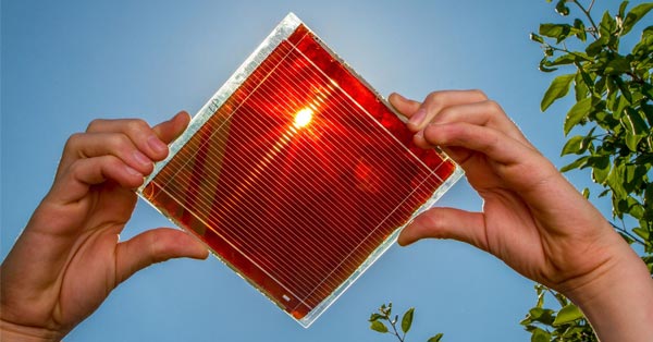
· More Iodine (I-rich): Narrower bandgap, close to 1.5 eV. The material appears black, absorbing a wide spectral range, suitable for single-junction cells.
· More Bromine (Br-rich): Wider bandgap, can be pushed to 2.3 eV. The material color becomes lighter, appearing reddish-brown or even yellow.
· Precise Ratio: To work with crystalline silicon in a tandem cell (where silicon absorbs red light), we need a top-layer material with a bandgap of about 1.68 eV - 1.75 eV.
Absorbs Light with Just a Thin Layer
Perovskite is a direct bandgap semiconductor; its hunger for light is much stronger than that of crystalline silicon.
· Absorption Coefficient: Perovskite's absorption coefficient is as high as the 10^5 /cm order of magnitude.
· Thickness Comparison:
o Crystalline Silicon: Because it is an indirect bandgap, light needs to travel a long way to be half-absorbed, so wafer thickness is usually 130 microns - 150 microns.
o Perovskite: Only needs a thickness of 500 nanometers (0.5 microns) to absorb more than 95% of visible light.
· Material Savings: To make batteries of the same area, perovskite's consumption of active material is only a few hundredths of that of crystalline silicon.
Manufacturing Batteries Like Printing Newspapers
Crystalline silicon requires high temperatures of 1400°C for crystal pulling, consuming huge amounts of electricity.
Perovskite manufacturing processes are completely different; it is "Solution Processing".
· Coating Process: Just like painting or printing a newspaper. The prepared perovskite precursor solution (ink) is coated onto glass or a substrate, then heated to 100°C - 150°C to dry and crystallize. The energy consumption of the whole process is extremely low.
· Equipment Cost (CAPEX): The investment for building a perovskite production line is about 50 - 80 million RMB/GW, while crystalline silicon lines usually require 150 - 200 million RMB/GW.
· Mainstream Methods:
o Spin Coating: Common in labs, suitable for small areas the size of a fingernail, achieving extremely high uniformity.
o Slot-die Coating: The choice for industrialization, suitable for large-area continuous production, but ensuring the crystallization uniformity of the thin film over a large area is a huge process difficulty.
o Evaporation: Similar to OLED manufacturing processes, evaporating materials onto the substrate in a vacuum.
"Lazy" Material That Tolerates Defects
In crystalline silicon, purity must reach 9N (99.9999999%); even a tiny bit of impurity ruins the cell.
· Defect Tolerance: Perovskite is a polycrystalline material containing many grain boundaries and defects. However, in the unique band structure of perovskites, these defects are mostly "Shallow Defects"; they don't latch onto electrons like deep-level traps to cause recombination.
· Low Purity Requirements: The raw material purity for manufacturing perovskite batteries usually only needs to be 99.5% - 99.9%, without expensive purification steps.
Trouble Brought by Soft Lattice
The structure of perovskite is maintained by weak chemical bonds (such as hydrogen bonds, ionic bonds), known as a "Soft Lattice". This makes it easy to process but also makes it extremely fragile.
· Fear of Water and Oxygen: Water molecules easily invade the crystal lattice, dissolving methylammonium (MA), causing the crystal structure to collapse and decompose into yellow lead iodide (PbI2).
· Fear of Heat: Even without water, organic modules easily evaporate when running for long periods at 85°C (IEC standard test temperature). This is currently the biggest obstacle to passing the IEC 61,215 standard test.
· Ion Migration: Under the action of an electric field, ions in the perovskite (especially iodine ions) run around inside the crystal like vagrants.
Efficiency Loss in Large Area Preparation
The efficiencies of over 26% you see reported in the news are usually measured on batteries of 0.1 square centimeters (grain of rice size). Once the area is enlarged, efficiency drops.
Area Classification | Typical Area | Typical Highest Efficiency (as of 2025) | Main Causes of Loss |
Cell | < 1 $cm^2$ | > 26% | Laboratory fine control, spin coating process, almost defect-free. |
Mini-module | ~800 $cm^2$ | ~20% - 22% | Uneven coating, dead area losses caused by laser scribing. |
Commercial | > 1.6 $m^2$ | ~16% - 18% (Pure Perovskite) | Large-area thin film resistance increase, pinhole defect probability rises exponentially. |
Lead Toxicity Issue
Perovskites contain Lead (Pb).
· Lead Content: Although the perovskite layer is only 500 nanometers thick, the lead content per square meter of module is about 0.4g - 0.7g.
· Leakage Risk: The real problem is lead solubility. Once perovskite decomposes upon contact with water, the lead ions inside dissolve very easily in water and seep into the soil.
· Solution: Must adopt physical and chemical dual-barrier encapsulation technologies, or even add lead-absorbing agents into the encapsulation film to lock lead ions immediately upon breakage.
Stability
According to the IEC 61,215 international standard, crystalline silicon modules generally offer a power warranty of 25 to 30 years.
Their T80 lifespan in actual outdoor operation often exceeds 30 years, with an average annual degradation rate controlled at 0.4% to 0.7%.
In contrast, Perovskite (PSC) belongs to ionic crystals. In the "Double 85" aging test at 85°C / 85% relative humidity, unencapsulated devices usually fail within hours.
Currently, the most advanced encapsulated perovskite devices have achieved thousands of hours of continuous operation under the ISOS-L-1 standard, but compared to the tens of thousands of hours of stability of silicon-based technology, there is still a gap of 1 to 2 orders of magnitude.
Silicon Durability
Atoms Connected Very Tightly
The fundamental reason why crystalline silicon batteries can sit there for decades without breaking lies in the way silicon atoms connect.
Silicon is located in Group IV of the periodic table; each silicon atom has 4 electrons in its outermost layer.
In the crystal structure, every silicon atom shares electrons with four surrounding silicon atoms, forming covalent bonds.
The binding energy of this covalent bond is about 226 kJ/mol (kilojoules per mole). This value is very large, requiring extremely high energy to break them apart.
In nature, ordinary sunlight irradiation, rain washing, or common air oxidation simply do not have enough energy to break this chemical bond.
In comparison, the binding force of many organic materials or ionic crystals (like perovskites) is much weaker; they fall apart with just a little moisture or heat.
Silicon's tetrahedral diamond structure determines from the physical bottom layer that it is not only hard but also chemically extremely inert.
Decades of Real Records
The National Renewable Energy Laboratory (NREL) in the US conducted a statistically massive study covering over 50,000 photovoltaic module systems globally.
Data shows that for monocrystalline silicon modules produced after 2000, the Median Degradation Rate is only 0.5% per year.
A module nominally rated at 400W, after 20 years of wind and rain outdoors, theoretically maintains an output power of around 360W (i.e., 90% of initial power).
Even more interesting are some antiques installed in the 1980s. For example, the TISO 10 kW system in Lugano, Switzerland, installed in 1982, used early Arco Solar silicon modules.
After running for 35 years, tests found that its average power still retained over 80% of the initial value.
These modules experienced decades of winter and summer heat cycles, yet the silicon wafers themselves underwent almost no essential physical degradation.
The main power losses instead came from the surface glass getting dirty, reduced light transmittance, and increased resistance at cable connections.
What Breaks is Usually Not the Cell
When we say "the solar panel is broken" or "the solar panel has aged," in 90% of cases, it doesn't mean the silicon wafer inside is broken, but that the materials wrapping the silicon wafer couldn't hold up.
The silicon wafer itself is a thin, brittle slice. To make it usable, factories encapsulate it like a sandwich: covered with a layer of glass on top, filled with EVA film in the middle, and a plastic backsheet on the bottom.
· EVA Film Yellowing: Under long-term UV irradiation, EVA film may decompose to produce acetic acid, causing the film to turn yellow. Yellow film blocks light, leading to less light received by the cell and reduced current.
· Backsheet Cracking: Early plastic backsheets easily became brittle and cracked in areas with large day-night temperature differences, allowing moisture to penetrate.
· Ribbon Fatigue: Cells are connected by tin-coated copper ribbons. Expanding by day and contracting by night, this repeated stretching loosens the weld points between the ribbon and the silicon wafer, increasing contact resistance.
In these failure cases, even if you disassemble the module, take out the silicon wafer, clean it, and retest it, its photoelectric conversion efficiency is often nearly the same as when it left the factory decades ago.
Physical Confidence Against Heat
The melting point of silicon is as high as 1414°C.
Of course, PV modules cannot work at the melting point, but this extremely high physical ceiling means the lattice structure of silicon atoms will not undergo thermal decomposition or phase change at any natural temperature on Earth.
Semiconductors all have a parameter called "Intrinsic Carrier Concentration."
As temperature rises, this concentration increases exponentially, causing cell leakage.
For silicon (bandgap 1.12 eV), this leakage effect is completely controllable below 200°C.
In comparison, Germanium (Ge) batteries collapse in performance around 70°C.
Therefore, routine outdoor high temperatures for silicon only cause a temporary voltage drop; once the temperature falls back, performance recovers completely without leaving permanent "internal injuries."
The Only Physical Weakness is Brittleness
Although silicon is strong chemically and thermally, it has a distinct shortcoming mechanically: Brittleness.
The physical properties of crystalline silicon are close to glass or ceramic. It is hard and lacks ductility.
If you bend a silicon wafer forcefully, it won't deform like metal, but will break directly.
As wafers are made thinner to cut costs, this issue becomes more sensitive.
Bumps during transportation or stepping on them during installation can generate Micro-cracks invisible to the human eye inside the silicon wafer.
· Initial Stage: When micro-cracks first appear, they might not affect output at all because the silicon pieces on both sides of the crack are still touching.
· Deterioration Stage: After months of outdoor thermal expansion and contraction, cracks slowly open, causing parts of the silicon wafer to disconnect from the main circuit, forming "islands." The electricity generated in these areas cannot be transmitted out, not only losing power but potentially causing Hot Spots due to localized heat accumulation, burning the backsheet.
Despite this, modern modules have mitigated this problem through Multi-Busbar (MBB) technology.
Even if the silicon wafer cracks, the dense metal wire mesh can conduct the current out like "needle and thread," ensuring the module isn't scrapped directly.
A Little Decay in the Initial Stage
Silicon-based batteries don't maintain perfect stability from day one. In the first few hours to weeks of use, a special phenomenon occurs called Light-Induced Degradation (LID).
This mainly occurs in boron-doped P-type monocrystalline silicon. Trace amounts of boron and oxygen atoms in the silicon wafer combine under light excitation to form a "Boron-Oxygen Complex."
This complex is a recombination center that eats up electrons, leading to a drop in efficiency.
Usually, this causes module power to drop by 1% to 2% in the first month.
Once the boron-oxygen complexes reach saturation, efficiency stabilizes and stops dropping rapidly.
Current N-type TOPCon batteries use phosphorus doping or gallium doping technology, eliminating this defect at the atomic level, making initial stability close to a perfect straight line.
Perovskite Weaknesses
Crystalline Silicon Efficiency Ceiling
The current highest laboratory efficiency record is about 26.8%, leaving less than 3% space from the 29.4% limit calculated by the Shockley-Queisser theory.
These last few percentage points are like improving a 100-meter sprint from 9.6 seconds to 9.5 seconds; every step forward requires fighting against basic physical laws.
Silicon Material Naturally Absorbs Light Slowly
Silicon belongs to indirect bandgap semiconductors, which is its biggest disadvantage at the physical level.
When photons are absorbed by direct bandgap materials (like Gallium Arsenide or Perovskite), electrons can transition and conduct electricity directly.
But in silicon atoms, electron transition requires not only absorbing photon energy but also changing momentum.
· Photon Penetration Depth: Because phonon cooperation is needed, the probability of silicon absorbing photons is greatly reduced. For longer wavelength red light, rays easily pass directly through the silicon wafer without being absorbed. To capture enough photons, crystalline silicon cell thickness must be maintained between 130 and 180 microns. In comparison, perovskite only needs 0.5 to 1 micron to absorb just as much light.
· Material Consumption: Maintaining thickness requires consuming large amounts of raw materials. Although wire sawing processes have made silicon wafers thinner and thinner, if thinner than 120 microns, mechanical strength drops sharply, making them extremely prone to fragmentation on automated production lines, causing yield losses.
Energy Wasted on Spectral Matching
Sunlight is a broad spectrum containing ultraviolet to infrared rays, while silicon's bandgap is fixed at 1.12 electron volts (eV). This value acts like a fixed-size sieve, only capturing energy of specific sizes.
Photon Type | Energy State | Result |
Low Energy Photons (< 1.12 eV) | Insufficient Energy | Infrared light with wavelengths greater than 1100 nm passes directly through the silicon wafer, making no contribution. This part accounts for about 19% of solar energy. |
High Energy Photons (> 1.12 eV) | Excess Energy | Blue light and UV light have high energy; after exciting electrons, the excess energy dissipates as phonons (heat) within a few picoseconds. This is thermalization loss, accounting for about 33%. |
Simply because of spectral mismatch, over 50% of solar energy is wasted the moment it enters the cell; this is locked by material properties and cannot be changed by processing.
Auger Recombination: The Physical Barrier
As cell efficiency gets higher, the internal carrier (electron and hole) concentration increases significantly.
At this point, a quantum mechanical phenomenon called "Auger Recombination" becomes a stumbling block.
At low concentrations, electrons and holes recombining and emitting light is normal.
But at high concentrations, the energy released by the recombination of an electron and a hole gets "intercepted" by another nearby electron.
This "third party" electron gains energy but does not output current, instead wasting the energy in the lattice through thermal relaxation.
· Doping Concentration Limit: To reduce resistance, the doping concentration of silicon wafers is usually increased. But the higher the doping, the greater the carrier density, and the probability of Auger recombination increases by the cube of the carrier density ($n^$3).
· Open Circuit Voltage Lock: Auger recombination directly limits the cell's open-circuit voltage (Voc). Currently, the Voc of PERC batteries hardly exceeds 690 mV. Even with the most advanced contact passivation technology, it is difficult to push Voc above 750 mV, while the theoretical limit is about 850 mV.
Mainstream Technology Routes Hit the Wall
Several mainstream technologies currently on the market each have their difficulties in approaching the limit:
1. PERC Technology (Passivated Emitter and Rear Contact)
· Status: This is the current market mainstay, with mass production efficiency between 23.5% and 24.5%.
· Bottleneck: The metal aluminum paste on the back of PERC cells directly contacts the silicon wafer, causing severe metal-induced recombination. This structure caps the efficiency limit around 24.5%; further improvements yield minimal returns on R&D investment, putting it on the edge of being eliminated by technological iteration.
2. TOPCon Technology (Tunnel Oxide Passivated Contact)
· Status: The next-generation technology taking over from PERC, with mass production efficiency about 25.5% to 26.2%.
· Bottleneck: It adds an extremely thin layer of silicon dioxide and polysilicon on the back. The problem is that this polysilicon layer itself absorbs light (parasitic absorption), especially short-wavelength light. This places an upper limit on current density (Jsc). Moreover, the firing process window for the front silver-aluminum paste is extremely narrow, making it difficult to ensure low resistance without damaging the underlying passivation layer. Its theoretical efficiency limit is about 28.7%, but actual mass production rarely exceeds 27%.
3. HJT/SHJ Technology (Heterojunction)
· Status: Extremely high efficiency, laboratory data can reach 26.8%.
· Bottleneck: It uses amorphous silicon thin films for passivation. Amorphous silicon not only absorbs light significantly but also has poor conductivity, requiring a transparent conductive film (TCO, usually Indium Tin Oxide ITO) on the surface.
o Scarcity of Indium: Indium is a rare metal with very low crustal abundance. If photovoltaics move towards Terawatt (TW) installation levels, global indium reserves simply won't be enough.
o UV Damage: The amorphous silicon layer is not resistant to UV rays; passivation effectiveness decays under long-term exposure.
Ion Mobility
Ions Running Around Inside
In traditional silicon-based solar cells, apart from electrons (negative charge) and holes (positive charge) running, other atoms are nailed to the floor, motionless.
But in perovskite, the situation is completely different.
Although it looks like a solid, under electric fields and light, the ions inside behave more like a "semi-liquid" or solid electrolyte.
This phenomenon is called Ion Migration. In the perovskite lattice, charged ions (mainly halogen anions like iodine ions I-) can easily detach from their original positions and drift long distances inside the crystal.
This is not just a theoretical physics problem; it is the main culprit directly causing unstable cell performance, inaccurate test data, and eventual device failure.
Low Threshold, Moves When It Wants
In physics, we use activation energy to measure how much energy an atom needs to jump to a neighboring vacancy.
· Iodine Ion (I-): Runs the fastest. Its migration activation energy is very low, usually between 0.08 and 0.3 eV. This is even lower than the diffusion barrier of ions in many liquid electrolytes.
· Methylammonium Ion (MA+): Runs a bit slower. As a large organic molecule, it is bulky to move, with activation energy around 0.5 to 0.8 eV.
· Lead Ion (Pb2+): Basically doesn't move. As the skeleton core of the lattice, lead ion activation energy usually exceeds 0.8 eV; under normal working conditions, its displacement is negligible.
Scan Data Doesn't Match Up
The most direct manifestation of ion migration is the Hysteresis Effect, which gave early researchers a headache because they found that the efficiency measured for the same cell was different.
When you measure the Current-Voltage (I-V) curve of a cell, you need to change the voltage to scan:
1. Reverse Scan: Sweep from Open Circuit Voltage (Voc) to Short Circuit Current (Jsc). At this time, the electric field established by internal ion distribution assists carrier extraction, and the measured efficiency is usually high.
2. Forward Scan: Sweep from Short Circuit Current (Jsc) to Open Circuit Voltage (Voc). Since the scan speed is usually faster than the speed of ion rearrangement, the previous ion distribution now becomes an obstacle, and the measured efficiency is usually low.
The faster the scan speed (e.g., 1,000 mV/s), the less time ions have to move, and hysteresis might look smaller;
If the scan speed is slow (e.g., 10 mV/s), ions run along with the voltage, and hysteresis becomes very obvious.
Splits Up As Soon As Light Hits
To adjust the light absorption range (bandgap) of perovskites, scientists often mix Iodine (I) and Bromine (Br).
This mixed-halide perovskite is peaceful in the dark, but once it encounters strong light, Photo-induced Phase Segregation (Hoke Effect) occurs.
· Separation Process: Under light, the lattice interior spontaneously splits into two regions. One region is enriched with iodine (I-rich), and the other is enriched with bromine (Br-rich).
· Energy Trap: The iodine-rich region has a narrower bandgap (lower energy level), acting like a trap to capture photogenerated carriers.
· Performance Consequence: The originally designed high voltage (based on mixed bandgap) suddenly drops, limited by that narrow-bandgap iodine-rich region.
Data monitoring shows that this separation usually happens between 10 to 100 seconds after illumination.
Although ions will slowly diffuse back and the material restores its original state after being placed in the dark for a while, in actual daytime continuous lighting environments, this separation persists, directly limiting the performance stability of wide-bandgap top cells in tandem batteries.
Blocking the Interface and Causing Damage
Ion migration isn't just tossing and turning inside the perovskite layer; they also accumulate at the interface between the perovskite and the Electron Transport Layer (ETL) or Hole Transport Layer (HTL).
This accumulation forms a very thin Debye Layer, usually only a few nanometers thick, but with huge impact:
1. Screening Electric Field: The direction of the electric field formed by ion accumulation is often opposite to the "built-in electric field" the cell uses to separate electron-holes.
2. Interface Recombination: Massive ion accumulation alters the energy band bending at the interface, creating numerous recombination centers. Electrons and holes run here and recombine/disappear before they can be collected by electrodes.
Weakness
Crystalline silicon cells are limited by the physical characteristics of indirect bandgaps.
Their photoelectric conversion efficiency is approaching the Shockley-Queisser theoretical limit of 29.4%, and they have a high temperature coefficient, with output power decreasing by an average of 0.3% to 0.45% for every 1 degree increase in operating temperature.
Their production requires high temperatures above 1400 degrees, resulting in high energy consumption, and the modules are rigid and fragile.
In contrast, perovskites face severe stability challenges. They are extremely sensitive to water and oxygen. In the IEC 61,215 standard aging test at 85 degrees / 85% humidity, they decay rapidly, and their T80 lifespan is far from reaching the 25-year standard required for commercialization.
Module efficiency is often 8% to 10% lower than laboratory small cells, and water-soluble lead leakage presents environmental compliance pressure.
Crystalline Silicon Efficiency Ceiling
Silicon Material Naturally Absorbs Light Slowly
When photons are absorbed by direct bandgap materials (like Gallium Arsenide or Perovskite), electrons can transition and conduct electricity directly.
But in silicon atoms, electron transition requires not only absorbing photon energy but also changing momentum.
There must be a "third party" involved, which is the phonon (lattice vibration).
· Photon Penetration Depth: Because phonon cooperation is needed, the probability of silicon absorbing photons is greatly reduced. For longer wavelength red light, rays easily pass directly through the silicon wafer without being absorbed. To capture enough photons, crystalline silicon cell thickness must be maintained between 130 and 180 microns. In comparison, perovskite only needs 0.5 to 1 micron to absorb just as much light.
· Material Consumption: Maintaining thickness requires consuming large amounts of raw materials. Although wire sawing processes have made silicon wafers thinner and thinner, if thinner than 120 microns, mechanical strength drops sharply, making them extremely prone to fragmentation on automated production lines, causing yield losses.
Energy Wasted on Spectral Matching
Sunlight is a broad spectrum containing ultraviolet to infrared rays, while silicon's bandgap is fixed at 1.12 electron volts (eV).
Photon Type | Energy State | Result |
Low Energy Photons (< 1.12 eV) | Insufficient Energy | Infrared light with wavelengths greater than 1100 nm passes directly through the silicon wafer, making no contribution. This part accounts for about 19% of solar energy. |
High Energy Photons (> 1.12 eV) | Excess Energy | Blue light and UV light have high energy; after exciting electrons, the excess energy dissipates as phonons (heat) within a few picoseconds. This is thermalization loss, accounting for about 33%. |
Simply because of spectral mismatch, over 50% of solar energy is wasted the moment it enters the cell; this is locked by material properties and cannot be changed by processing.
Auger Recombination: The Physical Barrier
As cell efficiency gets higher, the internal carrier (electron and hole) concentration increases significantly.
At this point, a quantum mechanical phenomenon called "Auger Recombination" becomes a stumbling block.
At low concentrations, electrons and holes recombining and emitting light is normal.
But at high concentrations, the energy released by the recombination of an electron and a hole gets "intercepted" by another nearby electron.
This "third party" electron gains energy but does not output current, instead wasting the energy in the lattice through thermal relaxation.
· Doping Concentration Limit: To reduce resistance, the doping concentration of silicon wafers is usually increased. But the higher the doping, the greater the carrier density, and the probability of Auger recombination increases by the cube of the carrier density ($n^$3).
· Open Circuit Voltage Lock: Auger recombination directly limits the cell's open-circuit voltage (Voc). Currently, the Voc of PERC batteries hardly exceeds 690 mV. Even with the most advanced contact passivation technology, it is difficult to push Voc above 750 mV, while the theoretical limit is about 850 mV.
Mainstream Technology Routes Hit the Wall
Several mainstream technologies currently on the market each have their difficulties in approaching the limit:
1. PERC Technology (Passivated Emitter and Rear Contact)
· Status: This is the current market mainstay, with mass production efficiency between 23.5% and 24.5%.
· Bottleneck: The metal aluminum paste on the back of PERC cells directly contacts the silicon wafer, causing severe metal-induced recombination. This structure caps the efficiency limit around 24.5%; further improvements yield minimal returns on R&D investment, putting it on the edge of being eliminated by technological iteration.
2. TOPCon Technology (Tunnel Oxide Passivated Contact)
· Status: The next-generation technology taking over from PERC, with mass production efficiency about 25.5% to 26.2%.
· Bottleneck: It adds an extremely thin layer of silicon dioxide and polysilicon on the back. The problem is that this polysilicon layer itself absorbs light (parasitic absorption), especially short-wavelength light. This places an upper limit on current density (Jsc). Moreover, the firing process window for the front silver-aluminum paste is extremely narrow, making it difficult to ensure low resistance without damaging the underlying passivation layer. Its theoretical efficiency limit is about 28.7%, but actual mass production rarely exceeds 27%.
3. HJT/SHJ Technology (Heterojunction)
· Status: Extremely high efficiency, laboratory data can reach 26.8%.
· Bottleneck: It uses amorphous silicon thin films for passivation. Amorphous silicon not only absorbs light significantly but also has poor conductivity, requiring a transparent conductive film (TCO, usually Indium Tin Oxide ITO) on the surface.
o Scarcity of Indium: Indium is a rare metal with very low crustal abundance. If photovoltaics move towards Terawatt (TW) installation levels, global indium reserves simply won't be enough.
o UV Damage: The amorphous silicon layer is not resistant to UV rays; passivation effectiveness decays under long-term exposure.
Perovskite Short Life
Fear of Water and Oxygen is Material Nature
Organic cations in perovskites (especially methylammonium MA+) love to absorb water extremely. This is not just physical adsorption, but irreversible chemical suicide.
· Extremely Fast Hydrolysis: Once air humidity exceeds 50%, water molecules can drill into the lattice structure. For methylammonium lead iodide, water molecules break the lead-iodine bond, decomposing the solid perovskite into liquid hydroiodic acid, methylamine gas, and solid lead iodide.
· Oxygen's Serial Destruction: In the dark, oxygen isn't that scary. But once there is light, oxygen molecules capture photogenerated electrons, turning into Superoxide.
Volatility and Phase Change Upon Heating
Crystalline silicon batteries just generate less power at 85 degrees, but perovskites may suffer structural collapse at 85 degrees.
· Volatility Issue: The commonly used methylammonium (MA) ion is highly volatile. At the standard aging test temperature of 85 degrees, MA ions decompose into gas and escape due to heat.
· Thermal Cycling Fatigue: The temperature difference between day and night outdoors is huge, 60 degrees by day and -20 degrees by night. Perovskite has a high thermal expansion coefficient, while the glass substrate or electron transport layer it attaches to has a low one.
Ions Running Around Inside the Cell
In crystalline silicon, atoms are fixed firmly. But in soft lattices like perovskite, iodine ions (I-) are attracted by light or electric fields and move inside the material like quicksand.
· Running Around by Day, Restoring by Night: While working during the day, ions accumulate at the electrode interface, forming a reverse electric field that cancels out the cell voltage. This leads to serious "Hysteresis Effect" in test data, where efficiencies measured by forward scan and reverse scan can differ by more than 10%.
· Corroding Electrodes: Escaped iodine ions don't just block the road; they also react with the top metal electrodes (gold, silver, copper). Silver iodide or copper iodide not only has poor conductivity but also diffuses further inward, causing the cell to short-circuit completely.
Ultraviolet Rays Become a Death Warrant
3% to 5% of sunlight is Ultraviolet (UV). Crystalline silicon is not afraid of UV, but the commonly used electron transport layer in perovskites (usually Titanium Dioxide TiO2) is extremely sensitive to UV.
Titanium dioxide is a photocatalyst. Under UV irradiation, it becomes extremely active, frantically snatching electrons from the perovskite surface.
This causes the perovskite material at the interface to decompose rapidly.
Although Tin Oxide (SnO2) can be used to replace Titanium Dioxide, or a UV cutoff film can be added to the glass, this sacrifices some short-wavelength photon absorption, effectively lowering the theoretical efficiency limit of the cell.
Reverse Bias is a Big Pit
In actual rooftop applications, it is inevitable that leaves or bird droppings block parts of the cells.
At this time, the blocked cell no longer generates electricity but becomes a load, bearing the reverse voltage poured in from other cells (Hot Spot Effect).
Crystalline silicon batteries can usually withstand reverse bias of 10 volts or even higher without damage, or be protected by bypass diodes.
But perovskites are extremely fragile. Many experiments show that a reverse bias of just -1 volt is enough to trigger an avalanche of ion migration, generating localized high heat and burning through the film directly.
Because perovskite heat dissipation is worse than silicon (low thermal conductivity), hot spots form extremely fast, often permanently physically damaging the cell before the bypass diode even has time to conduct.
Difficulty in Large Area Preparation
Spin Coating Doesn't Scale
Drop a drop of solution in the center of the glass and let the glass rotate at high speed, 4000 revolutions per minute.
Centrifugal force spreads the liquid extremely perfectly; excess liquid is thrown off, and the remaining film thickness is extremely uniform, with solvent evaporation speed consistent at the center and edges.
But in a factory, it is impossible to spin a large piece of glass of 2 square meters at several thousand revolutions; that would shatter the glass directly.
· Process Change: "Slot-die Coating" or "Blade Coating" must be used. This is like using a huge brush to paint on glass.
· Fluid Dead Corners: Without centrifugal force, liquid flow relies entirely on gravity and surface tension. As long as there is a speck of dust on the glass surface, or a one-micron vibration of the coating head, a long streak (Ribbing) will appear on the coating.
The Drying Process is Like Walking a Tightrope
The crystallization process of perovskite is extremely fast, often completed within a few seconds.
To ensure that quadrillions of crystal grains grow exactly the same over a large area, the difficulty is comparable to asking tens of thousands of people to stand up and sit down simultaneously without millisecond error.
· Coffee Ring Effect: When the solvent evaporates, the edges of the droplet evaporate faster, and the internal liquid flows to the edge, resulting in thick edges and a thin center (like a dried coffee stain). On a 1-square-meter large board, this uneven solvent evaporation leads to a pockmarked film surface like moon craters.
· Air Knife Quenching Challenge: To force the solvent to evaporate simultaneously, factories use a high-pressure nitrogen Air Knife to blow the wet film. The blowing force and angle of this "air knife" must be completely consistent within a 1-meter width. If the left side blows a bit harder and the right side a bit softer, the grains on the left will be very small, and the grains on the right will be very large.
Conductive Glass Resistance is Too High
Laboratory small batteries can use a whole piece of transparent conductive glass (ITO or FTO) as an electrode because the distance is short and resistance is negligible.
But if made into a 1-meter-long large cell, the resistance of the transparent electrode itself becomes startling.
· Resistance Loss: The sheet resistance of ITO is usually around 10 to 15 ohms. If the current has to run one meter on ITO, basically all the electrical energy is lost as heat on the way.
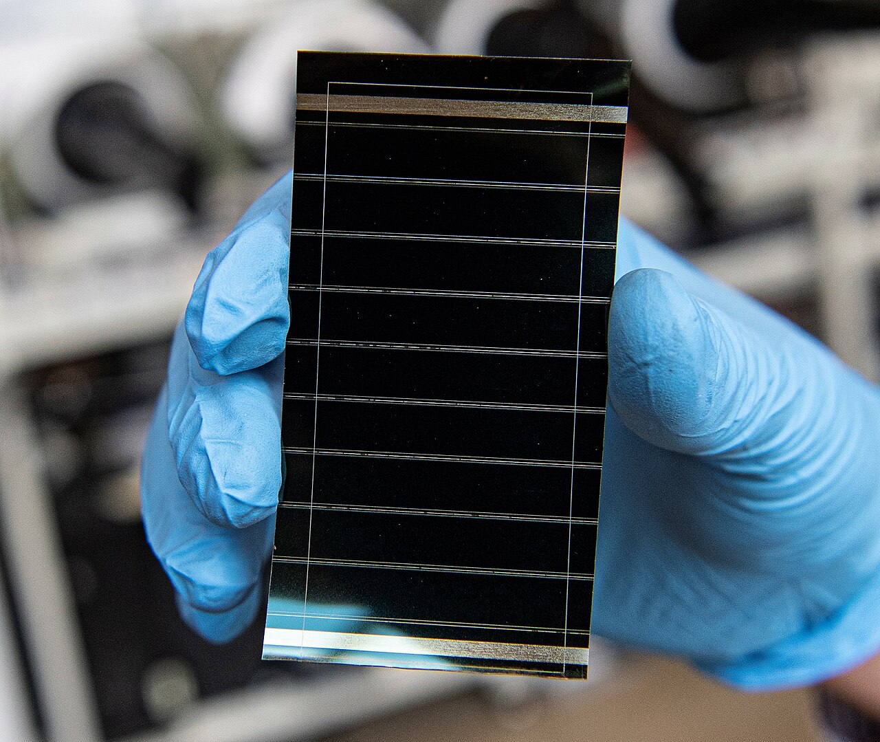
· Must Cut into Strips: To solve this problem, a whole large cell must be cut into dozens or even hundreds of long, thin small strips (Sub-cells) using lasers, and then connected in series like train cars. This way, the current only needs to run a short distance of 5 to 10 millimeters to enter the metal electrode.
Laser Scribing Must Be Extremely Precise
Cutting a large cell into small strips and connecting them in series requires precision laser scribing processes, termed P1, P2, P3 processes in the industry.
· P1 Scribing: Cuts the bottom transparent conductive layer to isolate each small cell.
· P2 Scribing: Cuts away the perovskite layer so the top metal electrode can flow down and contact the bottom conductive layer, achieving series connection.
· P3 Scribing: Cuts the top metal electrode to complete final isolation.
With these three cuts, the positional deviation of each cut cannot exceed 20 microns.
· Dead Area: The area between the P1, P2, and P3 lines generates absolutely no electricity; this is called "Dead Area." If the laser equipment is not precise enough, engineers can only leave a larger distance between lines to prevent cutting errors. This results in 5% or even 10% of the entire module area being "waste land," directly dragging down the Geometric Fill Factor (GFF) and final efficiency.
· Damage Risk: If laser heat is not controlled well, it will burn the perovskite material at the cut edge, leaving a large number of defects.
Probability of Pinhole Defects Explodes
On a 1 square centimeter small cell, the probability of a Pinhole appearing is very low; even if there is one, you just scrap that piece and get another.
But on a 20,000 square centimeter large module, requiring this entire layer of 500-nanometer thick film to not have a single pinhole is a statistically impossible task.
Defect Type | Consequence | Magnification Effect |
Tiny Pinhole | Top and bottom electrodes contact directly, causing a short circuit. | In a small cell, it might just be leakage. In a large module series structure, a short circuit in one sub-cell blocks the current of the entire string, forming a severe "short bucket effect," causing the power of the entire module to go to zero or generate significant heat. |
Thickness Fluctuation | Local uneven color, inconsistent resistance. | Causes uneven internal current flow, easily forming Hot Spots in thin areas, accelerating material decomposition. |
Layers Hard to Bond
Perovskite batteries usually have a 5 to 6 layer structure. Every layer must be stacked perfectly over a large area.
Especially the Hole Transport Layer (HTL), commonly used materials (like Spiro-OMeTAD) are very expensive and difficult to coat uniformly over large areas.
If 1% of the area between two layers is not bonded well, causing delamination or bubbles, charge cannot pass through.
In large-size processing, the physical contact stability of these interlayer interfaces is far harder to control than in small sizes, and delamination is extremely prone to occur during the subsequent lamination encapsulation process.