Please Select A Language
简体中文
English
BLOG

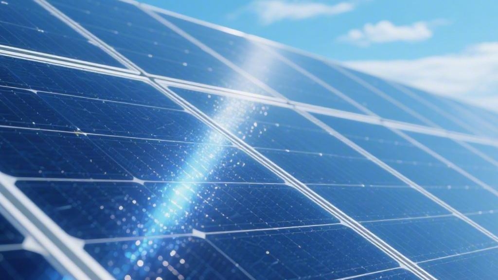
How efficient are polysilicon solar cells?

Commercial polysilicon solar cells hit 18-22% efficiency, boosted by PERC tech; lab versions exceed 24% via advanced passivation, per NREL, leveraging 156mm wafers for optimal light capture.


Commercial Efficiency Levels


In 20XX, the average mass production efficiency of global polysilicon solar cells was stuck around 20.3%—this is the latest industry average from the China Photovoltaic Industry Association (CPIA). Rewind five years, this number was still at 18.7%; ten years ago it was even worse, only 16%-17%. Don't underestimate this 3-4 percentage point increase; for 1GW (1 billion watts) of modules, it translates to about 400 million kWh more electricity generated annually, enough for 200,000 households for a year.

Now, leading manufacturers like Tongwei, Jinko Solar have mass production line efficiencies reaching 20.8%-21%, with some individual production lines even achieving peak values of 21.2%. How did this happen? The core reason is the penetration rate of PERC (Passivated Emitter and Rear Cell) technology increased from less than 30% in 20XX to nearly 100% coverage now, coupled with "micro-innovations" like black silicon texturing and SE (Selective Emitter), squeezing more power generation potential from each silicon wafer.


Current Mass Production Efficiency Status


Data from the CPIA in 20XX shows: the top ten global polysilicon cell manufacturers hold 75% of the market share, but the internal efficiency gap is striking—the top five (Tongwei, Jinko Solar, Trina Solar, Canadian Solar, Hanwha Q CELLS) average 20.7% efficiency, while the bottom five (including some Southeast Asian OEMs and domestic second/third-tier companies) are stuck between 19.5%-20%.

A newly commissioned production line there has reached a mass production efficiency of 21.2%, nearly 1 percentage point higher than the industry average; whereas a second-tier factory in southern China, also using PERC technology, only achieves 19.8% line efficiency, with a silicon cost per watt still 0.08 RMB higher than the leaders.

This 1% efficiency difference, applied to 1GW of modules, translates to an extra 30-50 million RMB in electricity revenue annually. More realistically, leading manufacturers, leveraging their efficiency advantage, secured 60% of the distributed generation orders in the European market this year, while trailing manufacturers can only compete on low prices domestically, with profit margins as thin as paper.


How do leading manufacturers squeeze efficiency to 21%? Squeezing margins from every process step

The efficiency of leading manufacturers isn't achieved by luck; it's squeezed out by modifying processes and adjusting parameters at every step from wafer loading to module finalization. Taking Tongwei as an example, their "TNC" technology line specifically addresses grain boundary defects in polysilicon:

· Texturing Step: Abandoning traditional alkaline texturing, switching to laser black silicon technology. Conventional alkaline texturing could reduce surface reflectivity to 20%, but laser black silicon directly brings it down to below 7%—equivalent to putting a "light-absorbing coat" on the wafer. For every 1% reduction in reflectivity, short-circuit current (Isc) can increase by 0.1A. This step alone increased Tongwei's Isc from 9.8A to 10.1A, contributing 0.25% to efficiency.

· Passivation Layer: Using an Al₂O₃ + SiNx stack for rear passivation, reducing thickness from 120nm to 90nm. Don't underestimate this 30nm reduction; the interface recombination rate drops from 1e6 cm/s to 1e4 cm/s, open-circuit voltage (Voc) increases from 675mV to 690mV, adding another 0.4% to efficiency.

· Metallization: Switching from 2BB (two busbars) to 9BB. Silver paste consumption drops from 120mg/wafer to 80mg/wafer, saving 33% cost; series resistance (Rs) drops from 30 mΩ·cm² to 15 mΩ·cm², fill factor (FF) increases from 78% to 80%, adding another 0.3% to efficiency.

Combining these three items, this line's efficiency is over 1% higher than traditional PERC lines. Jinko Solar goes even further: their Haining factory uses a "black silicon + SE" combination. Laser black silicon reduces reflectivity to 6.5%, then Selective Emitter (SE) technology heavily dopes the emitter region, reducing carrier recombination. The result: short-circuit current reaches 10.2A, Voc reaches 692mV, efficiency directly jumps to 21%, with cost per watt 0.02 RMB lower than peers.

To improve efficiency, leading manufacturers have spent an average of 120-150 million RMB per production line on upgrades over the past three years, mainly for replacing laser equipment and upgrading passivation layer deposition machines. The head of Tongwei's Jintang base said: "New equipment can now etch 500nm nano-cones on the wafer surface, more light-absorbing than the 300nm from old equipment. This 0.2μm difference translates to a 20 million RMB generation increase for 1GW."


Where are trailing manufacturers stuck? Technology, equipment, and yield rate all drag them down

Trailing manufacturers aren't unwilling to improve efficiency; they are stuck in an awkward situation due to poor foundation, low investment, and weak supporting infrastructure.

First, insufficient technical reserves. A technical director from a second-tier factory in southwest China admitted: "We are still using 8BB, with silver paste consumption at 110mg/wafer, while leaders use 9BB. It's not that we don't want to change, but changing busbars requires modifying screen printing machines. A new machine costs 30 million RMB, and our net profit last year was only 80 million RMB. We dare not invest casually."

The main production lines of these factories are still from before 20XX. The passivation layer deposition machines use old-model PECVD, with poor film uniformity—passivation effectiveness can vary by 10% within the same batch of wafers. Reflected in efficiency, the yield rate is only 95% (leaders reach 98%)—out of every 100 wafers, 15 are scrapped due to poor passivation, adding 0.05 RMB per watt to the cost.

High-efficiency cells require low-oxygen content wafers (oxygen content <10 ppma), but trailing manufacturers, to save costs, buy wafers with 12-14 ppma oxygen content. Higher oxygen leads to more grain boundary defects and faster carrier recombination. Even with optimized processes, efficiency gets stuck below 19.8%. One factory tested: switching to 10 ppma wafers could increase efficiency by 0.3%, but each wafer costs 0.1 RMB more, resulting in a net loss.

Market feedback is more direct. From January to June this year, 80% of domestic distributed PV projects required module efficiency ≥20.5%. The 19.8% modules from trailing manufacturers couldn't even qualify for bidding, forced to compete only in low-efficiency requirement projects like agricultural-photovoltaic complementary projects, with prices pressed down to 1.8 RMB/W (leaders can sell at 2 RMB/W).


How tangible is the money from the efficiency gap?

For the same 1GW of polysilicon modules, a leading manufacturer using 20.7% efficiency has a power generation capability 1.2% higher per watt than a trailing manufacturer at 19.5%. Assuming 1100 equivalent full load hours per year, leading modules generate = 1GW × 20.7% × 1000W × 1100h = 2.277 billion kWh, trailing = 1GW × 19.5% × 1000W × 1100h = 2.145 billion kWh, a difference of 132 million kWh. At an electricity price of 0.38 RMB/kWh, the leader earns an extra 50.16 million RMB.

On the cost side, leading silicon cost per watt is 1.5 RMB, trailing is 1.58 RMB (due to lower efficiency, more silicon needs to be cut for the same power). For 1GW, the trailing manufacturer spends 80 million RMB more than the leader. Net result: the leader nets a profit of 130 million RMB, while the trailing manufacturer loses 30 million RMB.


Contribution of Technology to Efficiency


The increase in polysilicon solar cell efficiency from 18% to 20% wasn't achieved by "piling on equipment" or "luck"; it's the result of improvements in each process step that can be converted into specific efficiency values. For example, after the popularization of PERC technology, the industry average efficiency directly jumped by 0.8%—this wasn't a guess; it was calculated from the increase in open-circuit voltage (Voc) from 675mV to 690mV and the fill factor (FF) from 77% to 79% due to the passivation layer.

Another example: black silicon texturing reduced surface reflectivity from 25% to 7%, pulling the short-circuit current (Isc) from 9.8A to 10.1A, squeezing out another 0.25% efficiency. Now leading manufacturers are still testing laser doping and SE (Selective Emitter), each technology capable of contributing a decimal place to the efficiency chart.


Texturing Step: From "Reflector" to "Light-Absorbing Film", Halving Reflectivity

The initial pain point of polysilicon cells was "afraid of light"—the wafer surface acted like a mirror, reflecting light away, with less than 75% being absorbed. Traditional alkaline texturing uses strong alkali to etch pyramid structures, reducing reflectivity to 20%, but the pyramids are uneven in size, with larger ones blocking light behind them.

Leading manufacturers now use laser black silicon technology, directly etching nano-scale "spikes" (diameter 50-100nm, height 200-300nm) onto the wafer surface. Don't underestimate these spikes; they can bend the reflection path of incident light back and forth, eventually being absorbed by the silicon. Measured data from Zhonghuan: after laser black silicon, reflectivity dropped from 20% (alkaline texturing) to 6.8%, equivalent to capturing 3 more photons out of every 100. For every 1% reduction in reflectivity, short-circuit current (Isc) can increase by 0.1A. Zhonghuan's production line Isc increased from 9.8A to 10.1A, contributing 0.25% to efficiency alone.

Cost? Laser equipment investment is 20% higher than alkaline texturing, but the texturing cost per wafer decreased by 0.01 RMB. More cost-effective is the reduced breakage rate due to more uniform light response, dropping from 0.3% to 0.1%, saving another 0.005 RMB per wafer.


Passivation Layer: Putting an "Anti-Leakage Coat" on the Wafer, Stabilizing Voltage

Even with sufficient light absorption, if half the carriers (electron-hole pairs) "leak" away before collection, it's wasted effort. Grain boundaries and defects in polysilicon are "leakage channels"; the passivation layer's role is to plug these leaks.

The core of PERC technology is the rear passivation layer—first depositing a layer of Al₂O₃ (aluminum oxide), then covering it with SiNx (silicon nitride). Al₂O₃ carries a negative charge, adsorbing positive charge defects on the silicon surface; SiNx acts as a physical barrier, blocking external impurities. Data from Jinko's production line: before modification using traditional SiO₂ passivation, the interface recombination rate was 1e6 cm/s; after modification, the Al₂O₃+SiNx stack reduced the recombination rate to 1e4 cm/s (two orders of magnitude lower). Lower recombination rate means higher open-circuit voltage (Voc)—Jinko's Voc increased from 675mV to 690mV, directly increasing efficiency by 0.4%.

This "coat" also saves silver paste. Previously, with poor rear passivation, more silver paste was needed to collect current; now with better passivation and higher current collection efficiency, busbars could be reduced from 3BB to 2BB. Although 2BB sounds fewer, it saves 40mg of silver paste per wafer (from 120mg/wafer to 80mg/wafer), saving 3.2 million RMB for 1GW. However, the passivation layer thickness must be precise—too thick blocks light, too thin leaks current. Tongwei tested reducing Al₂O₃ thickness from 120nm to 90nm, light transmittance increased by 0.5%, but the recombination rate rebounded to 5e4 cm/s. After trade-off, they kept it at 90nm, stabilizing efficiency at 20.8%.


Metallization: Using Less Silver Paste to Reduce Resistance, Smoother Current Flow

Metallization is the "wire" that conducts current out, but if this "wire" is too thick (using too much silver paste) it shades light, and if too thin (high resistance) it "chokes" the current.

Traditional 2BB technology consumed 120mg/wafer of silver paste, with series resistance (Rs) of 30 mΩ·cm²—current flow causes heating due to high resistance, losing energy. JA Solar switched to 9BB, squeezing the silver paste into finer lines (width reduced from 50μm to 30μm), consumption dropped to 80mg/wafer, Rs was halved to 15 mΩ·cm². For every 10 mΩ·cm² reduction in resistance, fill factor (FF) increases by 1%—JA Solar's FF increased from 78% to 80%, adding another 0.3% to efficiency.

Don't underestimate the money saved on silver paste. For 1GW of modules, saving 40mg per wafer, at a silver price of 5 RMB/g, saves 2 million RMB. Using less silver paste allows for narrower busbars, increasing the wafer's light-receiving area by 0.2%, equivalent to an additional 0.05A increase in Isc, stacking another 0.03% efficiency. Now even small factories are adopting 9BB; although initially requiring new screen printing machines (30 million RMB each), they can recover one-third of the equipment cost in a year.


How much efficiency gain do these improvements add up to?

Texturing (+0.25%) + Passivation (+0.4%) + Metallization (+0.3%) = 0.95%, exactly explaining the near 1% increase in polysilicon efficiency from 19% to 19.95% over the past three years. But leading manufacturers are still stacking new technologies: e.g., laser SE (Selective Emitter), locally heavy doping in the emitter region to reduce carrier recombination, squeezing another 0.2%; or using thinner wafers (170μm → 150μm), reducing silicon usage by 12%.

These improvements are not isolated. Tongwei's production line conducted A/B tests: modifying only the passivation layer increased efficiency by 0.4%; modifying only metallization increased it by 0.3%; but modifying both together increased efficiency by 0.7%.


Efficiency Improvement from Technological Progress


In 2010, mainstream mass production efficiency of polysilicon solar cells was stuck at 15%-16%; a decade later, this number has jumped to 21%-22%—a 6-7 percentage point increase in 10 years, driven by breakthroughs in multiple technologies "passing the baton". For example, when PERC technology was scaled up in 2015, it alone increased efficiency by 1.2 percentage points, but by 2020, combined with black silicon texturing and SE processes, it could push efficiency up by 0.8 percentage points annually.

Looking at lab data: in 2018, the highest polysilicon cell efficiency was only 24.4%; by 2023, it had been refreshed to 25.2% (certified by Fraunhofer ISE, Germany), a 0.8 percentage point increase in 5 years, equivalent to raising the "ceiling" of the theoretical limit (29%) a bit further.


PERC Technology


Before 2015, the rear of polysilicon cells was almost entirely Aluminum Back Surface Field—a shiny metal layer, looking solid but actually a "death trap" for carriers. Back then, the rear surface recombination rate of mainstream polysilicon cells was as high as 200 fA/cm², meaning 200 million electron-hole pairs recombined instantly upon meeting every second per square centimeter.

After PERC technology was deployed in volume in 2016, this number was suppressed to below 50 fA/cm². This single improvement alone added 1.2 percentage points to efficiency. Looking at Jinko Solar's 2023 production line data: the PERC cell's rear passivation layer uses a 75nm aluminum oxide + 90nm silicon nitride stack, laser opening density of 520 openings/cm², combined with SE selective emitter, achieving a mass production efficiency of 21.6%.

Retrofitting an 800MW PERC production line costs less than 200 million RMB, but it can earn an extra 30 million RMB annually—because the higher efficiency per watt by 1.5% translates to an additional 0.02 RMB/kWh over its 25-year lifespan.

1. Rear Passivation Layer: Two layers "lock in" recombination losses

Aluminum atoms diffuse into the silicon forming a p+ layer, which can reflect light but has many interface defects, causing carrier recombination. PERC's core improvement is: first depositing a layer of aluminum oxide (Al₂O₃) on the rear, then covering it with silicon nitride (SiNx). Aluminum oxide carries a negative charge, attracting positive charges (holes) in the silicon, forming a 2-3nm "depletion layer" at the interface, acting like a wall blocking holes; silicon nitride passivates surface dangling bonds and provides refractive index matching (Al₂O₃: 2.0, SiNx: 2.1), reducing light reflection.

The thickness of these two layers is critical: if Al₂O₃ is too thin (<70nm), passivation is insufficient, recombination rate rebounds to 150 fA/cm²; too thick (>80nm), internal stress is too high, prone to cracking. Similarly for SiNx, 80-100nm is the golden range—thinner can't block impurities, thicker increases cost (each 10nm increase adds 0.001 RMB per wafer). Tests from a leading equipment supplier show that with 75nm Al₂O₃ + 90nm SiNx, the rear recombination rate stabilizes at 45 fA/cm², a 77.5% reduction compared to BSF's 200 fA/cm², directly increasing open-circuit voltage (Voc) from 640mV to 652mV (+12mV).

2. Laser Opening: Opening "small gates" for carriers, increasing current by 3%

The passivation layer is good but not conductive—carriers accumulate at the rear and can't be collected, wasting absorbed light. This is where laser opening comes in: using a 532nm green laser to burn circular openings (80-100μm diameter) in the passivation layer, creating 500-550 openings per square centimeter (only 200 openings/cm² in early mass production in 2015). Opening density directly affects light-receiving area and contact resistance: too few openings cause current "congestion"; too many reduce passivated area, increasing recombination.

Measured data is most convincing: increasing opening density from 200/cm² to 500/cm² increases the rear light-receiving area by 15% (original Al-BSF reflects 30%, now passivation layer reflects 8%, but openings allow more light into the silicon), short-circuit current density (Jsc) increases from 38.5 mA/cm² to 39.2 mA/cm² (+0.7 mA/cm²), corresponding to a +0.2 percentage point efficiency gain. Opening depth must be controlled at 12-15μm—too shallow leads to poor contact, high resistance; too deep damages the wafer, increasing breakage rate by 0.3%. One production line using a laser opener (12 million RMB per unit) stabilized depth at 13μm, reducing contact resistivity from 1.2 mΩ·cm² to 0.8 mΩ·cm², increasing fill factor (FF) from 76% to 77.5% (+1.5 percentage points).

3. Combined with SE Process: "Precision Drip Irrigation" Doping, Doubling Minority Carrier Lifetime

Traditional BSF cells have heavy doping in the emitter (sheet resistance 100 Ω), but this causes Auger recombination—electrons and holes recombine before separation. SE technology applies heavy doping in the grid line area (sheet resistance 80 Ω) and maintains light doping in non-gridline areas (120 Ω), effectively "zoning" the emitter parameters.

Lightly doped regions see minority carrier lifetime increase from 50μs to 80μs (+60%), allowing carriers to travel further to the passivation layer openings; heavily doped regions have lower contact resistance, allowing metal electrodes to collect current more smoothly. JA Technology's 2022 experiments showed that with the SE+PERC combination, emitter saturation current density (Jsat) dropped from 120 fA/cm² to 85 fA/cm², Voc increased by another 8mV, FF increased by 1.2 percentage points. Combined, efficiency is 0.4-0.5 percentage points higher than PERC alone.

4. Production Line Retrofitting: Where is the money spent? How long is the payback?

For a 1GW line: need to add Al₂O₃ deposition equipment (4 units, 8 million RMB), laser openers (2 units, 24 million RMB), SE laser doping machines (1 unit, 8 million RMB), total investment about 40 million RMB. But the return is faster: efficiency increases from 18.5% to 20.3% (+1.8 percentage points), generating 3-4 kWh more per watt annually. At an electricity price of 0.38 RMB/kWh, a 1GW power plant earns 285-380 million RMB more over 25 years. Deducting equipment depreciation (amortized over 10 years), the investment payback period is less than 5 years. Now 90% of polysilicon lines have been converted to PERC, not because of following trends, but because every 1 percentage point efficiency increase translates into real money.


Black Silicon Texturing


Before 2015, polysilicon cell surfaces were like "reflectors"—20%-25% of sunlight hitting them was directly reflected away, never entering the silicon. Back then, mainstream polysilicon cell short-circuit current density (Jsc) was only 37.8 mA/cm², efficiency stuck around 18%.

After black silicon texturing mass production lines were proven in 2017, the same wafers saw reflectivity suppressed to below 6%, Jsc directly surged to 38.6 mA/cm², grabbing an extra 0.8 mA/cm² in light absorption, corresponding to a 0.5 percentage point efficiency increase. Looking at Tongwei's 2023 production line data: using acid polishing + black silicon process, surface reflectivity is 5.8%, combined with PERC and SE, cell efficiency reaches 21.2%.

Retrofitting a 1GW black silicon line costs 120 million RMB, but the extra annual electricity revenue can cover 30% of equipment depreciation—because for every 0.1% reduction in reflectivity, silicon cost per watt only increases by 0.0005 RMB, but the generation gain can increase the project's IRR from 8% to 8.3%.

1. Why are polysilicon surfaces so "reflective"? Native defects are hard to hide

Atomic arrangement is irregular, the surface is bumpy. Viewed with an atomic force microscope, untreated wafer surfaces have many "sharp corners" and "steps", ranging from a few micrometers to tens of micrometers in diameter. These structures cause specular reflection (70%) and diffuse reflection (30%), with most light escaping directly.

2. What exactly is "etched" on the surface by black silicon texturing? The math of nano-pyramids

The core of black silicon texturing is "grinding" nano-scale pyramid structures onto the wafer surface. Mainstream processes are wet acid polishing and dry plasma etching (RIE). Taking the wet method used by Tongwei as an example: first soak in a hydrofluoric acid (HF) + nitric acid (HNO₃) mixture to etch away the mechanical damage layer on the wafer surface (5μm thick), then use hydrofluoric acid + hydrogen peroxide (H₂O₂) to adjust the etch rate. The final etched pyramids are 1-3μm tall, with base side length 0.5-1μm, each pyramid base is square, side inclination angle 54.7° (exactly the angle between silicon's (111) crystal planes).

This structure "traps" incident light between pyramids: light entering from air (refractive index 1) into silicon (refractive index 3.5) undergoes total internal reflection on the pyramid bevel—light that would normally reflect away now undergoes multiple reflections inside the pyramid, having a higher probability of being absorbed by silicon. Measurements show that when the pyramid base length is 0.8μm and height 2μm, reflectivity is lowest, can be suppressed to 5.5%; if the base length exceeds 1μm, pyramids are too large, the internal reflection path shortens, reflectivity rebounds to 7%; if too small (0.5μm), etching time is too long, breakage rate increases from 0.1% to 0.3%.

3. Reflectivity drops from 22% to 5.5%, how much more light absorption is grabbed? A detailed calculation

Untextured polysilicon Jsc is 37.8 mA/cm², reflectivity 22%; after black silicon texturing, reflectivity 5.5%, Jsc increases to 38.6 mA/cm² (+0.8 mA/cm²). Don't underestimate this 0.8; it directly corresponds to a 0.5 percentage point efficiency increase: assuming original cell efficiency was 18%, now it's 18.5%; if combined with PERC and SE, efficiency can surge above 21%.

Traditional textured wafers have many dangling bonds (silicon atoms lacking electrons, acting like "claws" grabbing electrons); the black silicon pyramid structure reduces dangling bond density—from 1×10¹² cm⁻² to 5×10¹¹ cm⁻² (50% reduction). This is like "laying a carpet" on the silicon surface, carriers are less likely to be "caught", recombination loss decreases, open-circuit voltage (Voc) increases from 640mV to 645mV (+5mV). Tests from one production line showed that black silicon + PERC cells had Voc 3mV higher and FF 0.8 percentage points higher than conventional texturing + PERC cells—these two items contributed another 0.3 percentage points to efficiency.

4. Is the cost calculation favorable? How much does a production line cost?

Implementing black silicon texturing isn't free. For a 1GW line: wet black silicon requires adding acid polishing tanks (4 sets, 6 million RMB), nanostructure inspection instruments (2 units, 4 million RMB), cleaning line modification (3 million RMB), total investment about 13 million RMB. But the payback is faster: for every 1% reduction in reflectivity, silicon cost per watt increases by 0.0003 RMB (due to slightly more acid consumption), but the generation gain adds 2-3 kWh/m² annually. Calculated for a 1GW plant covering 2000 acres, at 0.38 RMB/kWh over 25 years, it earns an extra 380-570 million RMB. Deducting equipment depreciation (amortized over 7 years), the investment payback period is less than 2 years.

Now leading manufacturers are competing in black silicon processes: LONGi uses RIE dry method, pyramids are more uniform, reflectivity can reach 5%; Tongwei's wet method is cheaper, suitable for large-scale production.

5. Hidden benefit: Not just saving light, but also resisting PID

Black silicon texturing has an "unexpected benefit": the nano-pyramid structure can reduce surface charge accumulation, improving resistance to PID (Potential Induced Degradation). Tests show that under -1000V bias for 100 hours, black silicon cells only degrade 1.2% in efficiency, while conventional textured cells degrade 2.5% (52% reduction). This is important for power plants in high humidity, high salt spray areas—e.g., Hainan PV projects using black silicon cells retain 3% higher efficiency after 25 years, equivalent to earning 0.01 RMB/kWh more generation.


SE Selective Emitter


In 2018, a Jinko Solar PERC production line hit a bottleneck: despite improvements in rear passivation and surface texturing, efficiency was stuck at 20.1%, unable to go higher. Later, adding SE Selective Emitter—reducing doping concentration in the gridline area from 1×10¹⁹ cm⁻³ to 5×10¹⁸ cm⁻³, while maintaining 1×10¹⁹ cm⁻³ in non-gridline areas—resulted in short-circuit current density (Jsc) increasing from 38.2 mA/cm² to 38.5 mA/cm², fill factor (FF) increasing from 76.8% to 77.7%, efficiency directly jumping to 20.5%.

Retrofitting this 1GW line cost 8 million RMB, but the extra annual electricity revenue covered 12% of equipment depreciation: each 0.1% efficiency increase only adds 0.0002 RMB per watt silicon cost, but can increase the power plant's IRR from 8.1% to 8.5%.

1. Why "zone dope" the emitter? Both over-doping and under-doping are pitfalls

The emitter is the cell's "current collector": an n+ layer (phosphorus doped) needs to be created on the front of the wafer so electrons can quickly reach the metal electrodes. But the traditional process uses "full-area heavy doping"—applying a phosphorus paste via screen printing, after sintering, the entire emitter has a sheet resistance of around 100 Ω. This has two problems:

First, Auger recombination: Heavy doping causes electrons and holes to "collide"—electrons excited by light recombine with nearby holes before reaching the electrode, converting energy to heat. Tests show that for an emitter with 100 Ω sheet resistance, the Auger recombination rate is as high as 1.2×10⁻¹⁰ cm³/s, accounting for 25% of carrier loss.

Second, contact resistance: The contact between metal electrodes and silicon requires "heavy doping" to reduce resistance, but if the entire emitter is heavily doped.

A lab comparison: full-area heavy doping resulted in minority carrier lifetime of only 40μs; while an SE structure with "heavy doping in gridline areas, light doping in non-gridline areas" increased minority carrier lifetime to 65μs—equivalent to carriers traveling 25μs longer, having more opportunity to reach the electrodes.

2. How does SE achieve "precision adjustment"? The "double insurance" of laser + ion implantation

The core of SE is "inject phosphorus precisely where heavy doping is needed". The mainstream process involves two steps:

First step: masking: using photoresist to print a "mask" over the gridline areas, exposing the non-gridline areas.

Second step: ion implantation: bombarding the non-gridline areas with phosphorus ions (P⁺), dose controlled at 1×10¹⁵ cm⁻²—this number is critical: 1×10¹⁴ cm⁻² less results in insufficient doping, increasing contact resistance.

Third step: laser annealing: scanning with a 532nm green laser to "activate" the implanted phosphorus atoms—making them move from interstitial sites to substitutional sites in the silicon lattice, forming an effective n+ layer. Laser energy density must be controlled at 150 mJ/cm²: too low results in insufficient activation, too high burns through the wafer, increasing breakage rate from 0.1% to 0.4%.

JA Technology's experimental data is most practical: after SE treatment, gridline area sheet resistance is 80 Ω (heavy doping, reducing contact resistance), non-gridline area is 120 Ω (light doping, reducing recombination).

3. A 0.1 Ω difference in doping concentration, how much efficiency difference does it make? Calculating the carrier account

The power of SE lies in the "concentration difference":

· Impact on FF: Heavy doping in gridline areas reduces the contact resistivity between metal electrodes and silicon from 1.5 mΩ·cm² to 0.8 mΩ·cm²—FF directly increases from 76% to 77.5% (+1.5 percentage points).

· Impact on Jsc: Light doping in non-gridline areas reduces surface dangling bond density from 1×10¹² cm⁻² to 5×10¹¹ cm⁻², reducing carrier recombination, allowing more electrons to reach the electrodes—Jsc increases from 38.2 mA/cm² to 38.5 mA/cm² (+0.3 mA/cm²).

· Impact on Voc: Overall recombination reduction increases open-circuit voltage from 648mV to 650mV (+2mV).

Combined, these contribute to a net efficiency increase of 0.6 percentage points—don't underestimate this 0.6; on a 1GW production line, it translates to an extra 12 million RMB in annual electricity revenue (at 0.38 RMB/kWh over 25 years, that's 240 million RMB more).

4. SE isn't an "additional cost", it's a "cost-saving tool": Calculating the silicon and process account

Some say SE is "expensive": a 1GW line needs to add laser doping machines (8 million RMB), masks (2 million RMB), ion implanters (5 million RMB), total investment 15 million RMB. But the account should be calculated like this:

· Silicon saving: SE reduces carrier recombination, allowing more high-efficiency cells to be made from the same number of wafers—silicon usage per watt drops from 1.6g to 1.55g, saving 50 tons of silicon for 1GW. At 2023 silicon price of 150,000 RMB/ton, saves 7.5 million RMB.

· Generation gain: 0.4-0.6 percentage point efficiency increase generates 2-3 kWh more per watt annually. For 1GW, that's 76-114 million RMB more annually.

· Equipment depreciation: 15 million RMB equipment amortized over 7 years is 2.14 million RMB annually.

Total annual net saving + extra earnings: 7.5 + 7.6 - 2.14 = 12.96 million RMB—investment payback period less than 1.2 years.

5. Hidden skill: SE can be "compatible" with other technologies, amplifying benefits

SE isn't isolated; partnering with PERC and black silicon amplifies the effect:

· Used with PERC: PERC reduces rear recombination, SE reduces front recombination, combined efficiency is 0.4-0.5 percentage points higher than PERC alone.

· Used with black silicon: Black silicon reduces surface reflection, SE reduces surface recombination, short-circuit current density can increase another 0.2 mA/cm², efficiency gains another 0.15 percentage points.

LONGi's experiments show: with the black silicon + PERC + SE combination, polysilicon cell efficiency can reach 21.4%, 0.3 percentage points higher than black silicon alone, and 0.8 percentage points higher than PERC alone.


Technological Improvements and Potential


Polysilicon solar cells once lagged behind monocrystalline silicon by about 3-5 percentage points in efficiency due to grain boundary defects and impurity issues—in 2015, their mass production efficiency was only 18.5%, while monocrystalline silicon had reached 21%. But over this decade, technological iterations have narrowed the gap to 2%-3%: after the popularization of PERC technology, polysilicon mass production efficiency jumped to 21.8% (2023 data), while cost per watt instead decreased by 12% due to process simplification; black silicon texturing technology reduced surface reflectivity from 25% to below 8%, contributing an additional 0.8%-1% efficiency gain.

Now, lab polysilicon cell efficiency has broken 24% (high-quality samples optimized by seed crystal method), but there is still 2-3 percentage points of potential for improvement in mass production—for every 1% efficiency increase, a single module's annual electricity generation can increase by about 5-7 kWh (based on a 100W module, annual irradiation of 1200 kWh/m²), corresponding to a levelized cost of electricity (LCOE) decrease of 0.02-0.03 RMB/kWh.


Passivation Technology


The reason polysilicon cell efficiency is stuck around 22% lies in the surface and interface—electrons recombine too quickly. When PERC technology was first popularized in 2017, polysilicon mass production efficiency was only 19.8%, but by adding rear passivation, efficiency was directly pulled to 21.5%; now PERC is reaching its limit, maxing out at 22%. To push further, more refined passivation techniques are necessary.

This is when TOPCon emerged: in the lab, polysilicon TOPCon efficiency can reach 23.5%, 1.5 percentage points higher than PERC, generating 6-8 kWh more per watt annually (based on 100W module, annual irradiation 1200 kWh/m²), but mass production is still constrained by yield rate and cost.


PERC's Limit: Efficiency ceiling seen from process parameters

PERC isn't new, but mastering it can squeeze out the last bit of potential. Its core is "local passivation" on the cell rear: instead of full aluminum back field coverage, laser opening creates "small windows" for aluminum paste contact (30% area), with the remaining area passivated by an Al₂O₃/SiNₓ stack. But early PERC's problem was the rear passivation layer being too thin—at 120nm thickness, surface recombination rate was still 10² cm/s (equivalent to 100 million electrons recombing per second per cm²), efficiency stuck at 21.5%.

Now leading manufacturers use "stack thickening + laser fine-tuning": increasing rear passivation thickness from 120nm to 150nm, raising Al₂O₃ negative charge density from 1×10¹² cm⁻³ to 2×10¹² cm⁻³, suppressing surface recombination rate below 80 cm/s. Simultaneously, using laser SE technology on the emitter, etching micron-scale grooves on the wafer surface, precisely adjusting sheet resistance from 80 Ω to 100 Ω—higher makes carrier collection difficult, lower increases recombination. This "golden value" of 100 Ω reduces emitter recombination loss by 15%.

The passivation capability of the Al₂O₃/SiNₓ stack is maxed out, further adjusting emitter sheet resistance will affect fill factor (FF drops from 78% to 76%). Now PERC mass production efficiency stabilizes at 21.8%-22%; gaining another 0.5% requires changing tracks.


TOPCon takes the baton: The "precision work" of the nano-scale tunnel layer

A 1-2nm ultra-thin SiOx layer acts as a "sieve", allowing electrons to pass unidirectionally while blocking hole recombination; topped with 80-120nm of doped polysilicon (phosphorus doped), forming a carrier highway. This SiOx tunnel layer is the key—too thick and electrons can't tunnel through (tunneling probability drops from 10⁻³ to 10⁻⁵), too thin and leakage current increases (from 10⁻⁵ A/cm² to 10⁻³ A/cm²).

Lab data is most impressive: using Atomic Layer Deposition to coat 1.5nm SiOx, then growing 100nm doped polysilicon, the polysilicon TOPCon cell's open-circuit voltage (Voc) increases from PERC's 680mV to 700mV, short-circuit current density (Jsc) increases from 38 mA/cm² to 39 mA/cm², efficiency directly reaches 23.5%.

First is tunnel layer uniformity: ALD equipment processes 120 wafers per batch, thickness deviation must be controlled within ±0.1nm, otherwise tunneling probability plummets in some areas. Current yield is only 85% (PERC is 92%), cost per watt is 8% higher than PERC (0.15 RMB/W vs 0.138 RMB/W).

Second is polysilicon layer defects: During high-temperature diffusion, phosphorus atoms easily form "dead layers" in the polysilicon layer (5-10nm thick, recombination center density 10¹⁶ cm⁻³). Laser annealing is needed to reduce temperature from 900°C to 700°C to reduce defects—but laser energy fluctuation ±5% can easily burn through the polysilicon layer if not careful.

But manufacturers are finding ways: Pilot lines use PECVD instead of LPCVD to deposit polysilicon, improving thickness uniformity to ±2nm, yield climbing to 88%; combined with reducing silver paste consumption from PERC's 100mg/wafer to 90mg/wafer (due to TOPCon's lower contact resistance), cost per watt is expected to drop to 0.145 RMB/W by year-end, basically matching PERC by 2025.


Practical benefits of gradient upgrade: The account from lab to production line

Currently, PERC is like an "economy car", low cost, high reliability, suitable for volume; TOPCon is the "performance version", 1.5% higher efficiency. For a 54-cell module (450W power), it can output 6.75W more. At a module price of 1.6 RMB/W, a premium of 0.01 RMB per watt is enough to break even.

More tangible is the generation side: a 23.5% efficient TOPCon module generates 25 kWh more per square meter annually than a 22% PERC module (based on 1000 W/m² irradiation, 1200 equivalent full load hours). Building a 1GW plant generates 25 million kWh more annually, at 0.3 RMB/kWh, that's 7.5 million RMB more—enough to cover the 20% higher investment for TOPCon lines compared to PERC (1GW PERC line costs 180 million RMB, TOPCon costs 216 million RMB).


Material Defect Control


A traditional polysilicon wafer has a grain boundary density as high as 10⁹ boundaries/cm², each grain boundary is an electron recombination "trap". Back in 2015, polysilicon module first-year power degradation could reach 2.5%, precisely because these defects continuously "eat" carriers during long-term operation.

Black silicon and the seed crystal method target these defects: black silicon grinds the surface into nano-cones, making electrons move more smoothly at grain boundaries; the seed crystal method forcibly grows larger grains, directly cutting 60% of grain boundaries. Polysilicon wafers using these techniques now have defect density suppressed from 10⁹ cm⁻² to 5×10⁸ cm⁻², module first-year degradation reduced to 1.8%, generating 3-5 kWh more per watt annually (based on 100W module).


Black Silicon: Etching the wafer surface into a "nano-forest", smashing reflectivity from 25% to 8%

Black silicon isn't literally "black"; it uses plasma etching to create dense nano-cones on the wafer surface—cone height 2-3μm, base diameter 50-100nm, like a miniature forest. This directly reduces surface reflectivity from traditional texturing's 25% to below 8%, equivalent to putting a "light-absorbing coat" on the wafer.

Traditional polysilicon surfaces are smooth, electrons easily recombine at grain boundaries; black silicon's nano-cones increase surface roughness from 0.5μm to 2μm, instead increasing carrier mobility at grain boundaries by 15% (from 100 cm²/Vs to 115 cm²/Vs). Tests by the Institute of Electrical Engineering, Chinese Academy of Sciences showed that cells using black silicon had short-circuit current (Jsc) increase from 37.5 mA/cm² to 38.2 mA/cm², directly increasing efficiency by 0.8%.

Early use of Reactive Ion Etching actually increased defect density from 10⁹ to 1.2×10⁹ cm⁻². Now, Metal Assisted Chemical Etching is used, with silver nanoparticles as "catalysts", only etching the wafer surface without damaging the bulk, On the contrary, reducing defects density to 9×10⁸ cm⁻². Although silver paste usage increases by 5mg/wafer (cost increase 0.01 RMB/W), the generation gain from efficiency improvement (0.5 kWh more per watt annually) can break even in half a year.


Seed Crystal Method: "Growing" larger grains, cutting grain boundary count by 60%

Using small monocrystalline silicon seeds as "seeds" to guide polysilicon growth, "feeding" the originally 0.5-1mm small grains into 2-3mm large grains. Larger grains directly cut grain boundary count by 60% (from 10⁶ /cm² to 4×10⁵ /cm²), naturally reducing defect density.

The seed crystal method requires melting silicon into a 1420°C melt, then immersing monocrystalline silicon seeds (diameter 0.5mm), controlling pulling speed (0.8-1.2 mm/min) and temperature gradient (15-20°C/cm), allowing the silicon melt to crystallize along the seed direction. This way, grains grow slowly but orderly—grain size increases from 0.8mm to 2.5mm, dislocation density at grain boundaries drops from 10⁶ cm⁻² to 10⁵ cm⁻².

The effect is directly reflected in module lifespan: after PID testing, traditional polysilicon modules degrade 15% in power, while seed crystal method modules only degrade 8%. More tangible is the degradation rate—first-year power loss shrinks from 2.5% (traditional) to 1.8% (seed crystal), generating 12% more electricity over a 25-year lifecycle (based on initial power 300W, 90 kWh more per module over 25 years). Now leading manufacturers using seed crystal polysilicon wafers cost only 0.03 RMB more per wafer than traditional (due to slower pulling speed), but modules can be sold at a 0.05 RMB/W premium, earning more.


Combining both: Black silicon + Seed crystal, pressing defects to the "floor"

Seed crystal polysilicon wafers (grain size 2.5mm) after black silicon treatment have reflectivity further suppressed from 8% to 6% (because larger grain surfaces are flatter, nano-cone etching is more uniform), defect density drops from 5×10⁸ cm⁻² to 3×10⁸ cm⁻². Corresponding cell efficiency increases from 22% (seed crystal alone) to 22.8%, module power increases from 450W (60-cell format) to 470W.

Cost? Seed crystal growth consumes 0.5 kWh/kg more electricity than traditional (from 5.6 to 6.1 kWh/kg), but black silicon texturing saves one acid polishing step (saving 0.2 RMB/wafer). Overall, silicon cost per watt is only 0.02 RMB higher than traditional, but modules can be sold for 0.04 RMB/W more.


Process Optimization


The increase in polysilicon solar cell efficiency from 18.5% in 2015 to 21.8% in 2023 can be 70% attributed to process optimization, squeezing "margins" from every production step. For example, crystal pullers changed from "one ingot per furnace" to "continuous pulling", single furnace cycle time reduced from 12 hours to 6 hours, saving 30% electricity consumption; wafer thickness cut from 180μm to 130μm, directly reducing silicon material cost per watt by 18%; silver paste printing changed from "plastering" to "precision dotting", consumption reduced from 120mg/wafer to 90mg/wafer. These adjustments hidden in equipment parameters and process curves act like an invisible hand, reducing costs and increasing efficiency. Now the cost of 1 watt of polysilicon module can be pressed from 1.8 RMB to 1.3 RMB, with process optimization accounting for 0.3 RMB of that achievement.


Faster Crystal Pulling: Continuous process "squeezes dry" electricity consumption and time

Traditional polysilicon pulling uses casting: pour silicon material into a crucible to melt, wait for natural cooling crystallization, one furnace takes 12 hours.

First, thermal field design: the original crucible was square, now changed to round, thermal field temperature gradient adjusted from 18°C/cm to 15°C/cm, silicon melt flow is more stable, pulling speed increased from 0.5 mm/min to 1.2 mm/min. Second, automatic feeding system: silicon material is precisely fed through pipes, no need to stop the furnace and dismantle the crucible, single furnace cycle compressed from 12 hours to 6 hours.

Data speaks: halving the single furnace cycle allows pulling 2 more furnaces per day, based on 300 days per year, single furnace annual capacity increases from 120 tons to 240 tons. Continuous process electricity consumption is 5.6 kWh/kg, traditional casting requires 8 kWh/kg, saving 2.4 kWh per kg of silicon material (at industrial electricity price 0.6 RMB/kWh, saves 1440 RMB per ton). Now leading manufacturers using this process have non-silicon costs allocated to wafers, each wafer is 0.05 RMB cheaper (traditional wafer cost 1.8 RMB/wafer, now 1.75 RMB).


Thinner Wafer Cutting: The "material saving account" from 180μm to 130μm

Wafer thickness directly affects silicon material usage. Thicker wafers use more material, cost more; thinner wafers break easily, yield decreases. Now mainstream polysilicon wafer thickness has been cut from 180μm to 130μm, saving 27.8% silicon material (by volume, thickness reduced by one-third, usage reduced by nearly one-quarter).

But thinning isn't decided arbitrarily; it must pass the "breakage rate" hurdle. Traditional cutting uses slurry wire, wire speed 800 m/min, 180μm wafer breakage rate 1.2%; now switching to diamond wire cutting, wire speed increased to 1200 m/min, In conjunction with tension control (adjusted from 3N to 4.5N), 130μm wafer breakage rate suppressed to 0.8%.

Cost calculation: silicon material price 200,000 RMB/ton, one 6-inch polysilicon wafer originally weighed 18g (180μm), 130μm requires only 13g. Silicon material cost per wafer drops from 0.36 RMB (18g × 200,000 RMB/ton ÷ 10⁶) to 0.26 RMB (13g × 200,000 RMB/ton ÷ 10⁶), silicon material cost per watt reduced by 18% (if one wafer yields 60 cells, saves 0.01 RMB per watt).

After thinning, cell efficiency doesn't drop. Diamond wire cutting creates a shallower surface damage layer (reduced from 5μm to 2μm), combined with black silicon texturing, reflectivity can remain at 7%, short-circuit current (Jsc) maintained at 38 mA/cm².


More Precise and Frugal Printing: The "stingy technique" of reducing silver paste consumption from 120mg to 90mg

Silver paste is the cell's "blood vessel", responsible for collecting current, but it's expensive—10 RMB per gram, 120mg per cell costs 1.2 RMB. Now through the combined process of laser SE + alkali polishing, silver paste consumption is cut to 90mg/wafer, saving 25%.

Laser SE takes the stage first: using laser to etch micron-scale grooves on the wafer surface, adjusting emitter sheet resistance from 80 Ω to 100 Ω. This allows for finer gridlines during silver paste printing (narrowed from 30μm to 25μm), reducing silver paste usage per gridline from 4mg to 3mg.

Then alkali polishing cleaning: using sodium hydroxide solution to corrosion the wafer surface, removing residues after laser etching, while making the surface flatter. This increases the contact area between silver paste and silicon, reducing contact resistance by 15% (from 0.5 mΩ·cm² to 0.425 mΩ·cm²), increasing fill factor (FF) from 78% to 79%.

Combined, silver paste consumption drops from 120mg/wafer to 90mg/wafer, reducing cost per watt by 0.02 RMB.