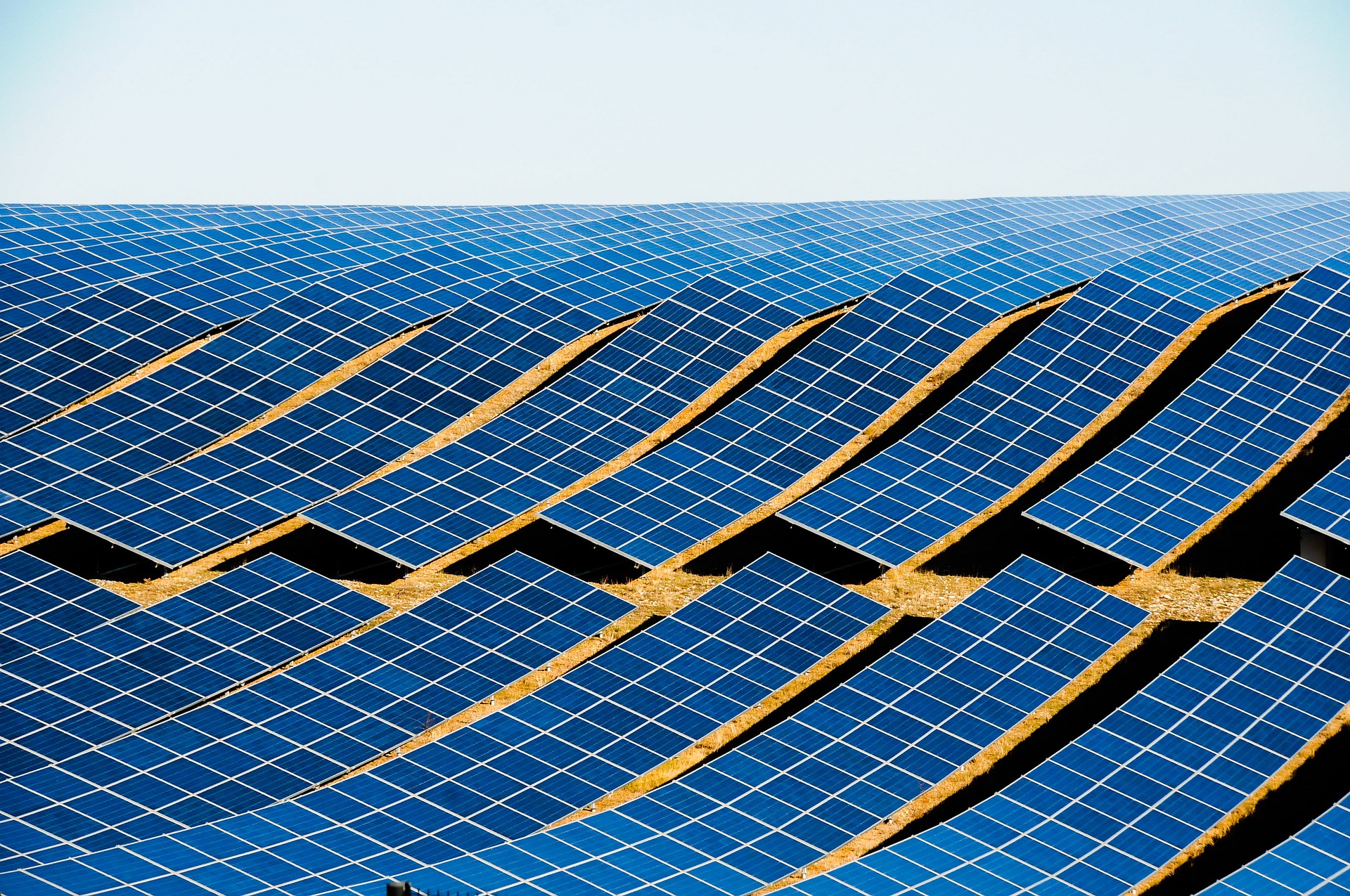
The Complete Guide to Thin-Film Solar Cells | Low-light Performance, Efficiency, Attenuation Rate
Thin-film modules offer excellent low-light performance, generating 5-10% more electricity than crystalline silicon on cloudy days.
Their biggest advantage is extremely slow degradation, with an initial degradation of about 2% in the first year, and only 0.4% annually thereafter, ensuring long-term energy yield.
However, their efficiency is relatively low (commercially 10-13%), requiring more installation area. They are more suitable for special applications sensitive to weight and low-light conditions.
Low-light Performance
When light intensity is below Standard Test Conditions (1000 W/m²), for example, in 200 W/m² morning light or overcast conditions, cadmium telluride (CdTe) modules can typically maintain over 83% of their rated power output, whereas the output of typical crystalline silicon modules may drop to 78%-80% of their rated value.
This difference stems from the material's inherent spectral response and lower temperature coefficient, allowing thin-film cells to have longer effective daily generating hours under real-world varying light conditions, potentially increasing total annual energy yield by 5-10%.
Definition
What exactly is "low light"?
It encompasses various daily scenarios with insufficient illumination:
l Low-intensity light: Early morning and dusk, where light intensity is typically between 200-400 W/m².
l Diffuse light: Overcast, cloudy, or hazy weather, where direct sunlight is scattered by clouds, water droplets, or particles in the atmosphere.
l Non-optimal angle light: When sunlight does not hit the panel perpendicularly, reducing the energy received per unit area.
Parameters quantifying low-light performance
The industry typically evaluates a cell's low-light performance by measuring its "relative efficiency" at different light intensities.
Specifically, it involves looking at the output power at conditions like 200 W/m², 400 W/m², 600 W/m², etc., as a percentage of the power under Standard Test Conditions.
Metric | Description | Example/Typical Value |
Low-light Response | The amount of current generated per unit light intensity. Higher responsivity means better startup and power generation capability under low light. | The quantum efficiency of thin-film cells in the 300-500nm blue-violet wavelength range can exceed 85%, superior to typical values for c-Si in this band. |
Fill Factor Retention | Fill Factor measures the "squareness" of the cell's I-V curve. Slower decline in Fill Factor under low light indicates more stable performance. | At 400 W/m², the Fill Factor of a high-efficiency CdTe thin-film module might drop only 3-5 percentage points from standard conditions, whereas a typical PERC c-Si cell might drop 5-8 points. |
Spectral Response Difference | Different technologies have varying sensitivity to different light wavelengths. The spectral distribution changes under low light, altering cell response. | On cloudy days, the proportion of blue light in the spectrum increases. Amorphous silicon thin-film cells absorb light in this band more effectively. |
Testing standards for low-light performance
The International Electrotechnical Commission (IEC) standard IEC 61,853-1 specifies procedures for photovoltaic module performance testing, including performance measurements at low irradiance levels.
This allows for standardized comparison of low-light performance between different products. For example, the standard requires measuring module performance at conditions like 200 W/m² and 800 W/m².
Relationship between low-light performance and peak efficiency
A module with a rated peak efficiency of 20% might perform far worse under low light than a module rated at 18% efficiency.
l Peak Efficiency is like asking about a sports car's top speed on a racetrack.
l Low-light Performance is like measuring a car's comprehensive fuel economy and driving smoothness in city traffic with congestion, curves, and frequent stops/starts.
For PV systems, the total annual energy generation (kWh) is far more important than the peak power (Wp).
Low-light performance directly determines the energy generated during non-ideal light periods, significantly impacting the total annual energy output.
According to analysis by the Fraunhofer Institute for Solar Energy Systems in Germany, under Central European climate conditions, differences in low-light performance can cause up to a 6% variation in a PV plant's annual energy yield.
Principle
More "tolerant" ability to capture light
The efficiency of a solar cell largely depends on the range of light wavelengths it can utilize.
Traditional crystalline silicon is an "indirect bandgap" semiconductor, requiring the combined action of photons and atomic vibrations to generate current. This leads to inefficient absorption of photons at certain wavelengths, especially in the blue-violet region under weaker light.
Thin-film materials (like CdTe, CIGS) are "direct bandgap" semiconductors.
Their ability to absorb photons is much stronger; even a very thin layer of material (1-3 microns, only about one-hundredth the thickness of c-Si) can effectively absorb most sunlight.
In low-light environments where photon flux density is low, this high light absorption characteristic becomes crucial, ensuring enough photons are captured and converted into electricity.
Data comparison:
CdTe has an absorption coefficient as high as 10⁵ cm⁻¹ in the visible light range, while c-Si's absorption coefficient is about 10³ cm⁻¹.
CdTe material can absorb over 90% of visible light at a thickness of just 1 micron, whereas c-Si requires over 100 microns thickness to achieve the same absorption.
"Eyes" better matched to the cloudy sky spectrum
When sunlight passes through clouds, the spectral composition changes: the proportion of long-wavelength direct light (red, infrared) decreases relatively, while the proportion of short-wavelength scattered light (blue, violet) increases.
l C-Si's Shortcoming: c-Si has a bandgap of about 1.1 electron volts (eV), with its spectral response peak in the infrared region. On cloudy days, the infrared light it is good at capturing decreases, while the proportion of blue-violet light it is less adept at increases, leading to a noticeable drop in overall conversion efficiency.
l Thin-film's Advantage: The bandgap of many thin-film materials can be tuned to better match the visible light spectrum. For example, CdTe's bandgap is about 1.45 eV, and CIGS's bandgap can be adjusted between 1.0-1.7 eV.
Quantum efficiency curves show that in the 400-500 nanometer blue light wavelength region, the quantum efficiency of high-efficiency CdTe cells can remain above 80%, while c-Si cell efficiency in this band is typically only 60-70%.
Lower "internal resistance"
Under low-light conditions, the current generated within the cell is very weak.
At this point, any losses caused by internal resistance become particularly prominent, severely affecting output voltage and power.
The structure of thin-film cells favors reducing such losses:
l Extremely short charge transport paths: Photogenerated charges (electrons and holes) generated within the micron-thin layer only need to travel a very short distance to be collected by the electrodes on the top and bottom.
l Better Fill Factor retention: Fill Factor measures how "square" the cell's output characteristic curve is. Under low light, the drop in Fill Factor for thin-film cells is typically smaller than for c-Si cells. For example, at 400 W/m² irradiance, the Fill Factor of a high-efficiency CdTe module might drop from 78% under STC to 75% (a drop of only 3.8%), while a typical PERC c-Si module might drop from 80% to 75.5% (a drop of 5.6%).
Less affected by temperature
Solar cells operate at temperatures far above the laboratory's 25°C in the real world. High temperatures reduce the cell's output voltage, leading to power loss. This negative effect is measured by the "temperature coefficient".
l C-Si cell temperature coefficient is typically between -0.3%/°C to -0.4%/°C. For every 1°C temperature increase, its output power decreases by about 0.3%-0.4%.
l Thin-film cell (especially CdTe) temperature coefficient is better, around -0.2%/°C.
Thin-film vs. Crystalline Silicon
Difference in the slope of low-light output curves
Under standard laboratory test conditions, a monocrystalline silicon module with 22% efficiency might output more power than a cadmium telluride module with 20% efficiency.
However, as light conditions deviate from the standard state, this relationship begins to change.
By analyzing the relative output (with STC output as 100% baseline) at different irradiance levels, two distinct decay curves can be plotted.
The output curve for c-Si drops more steeply, while the curve for thin-film is relatively flatter.
· At 800 W/m² (slightly cloudy bright weather), a high-efficiency monocrystalline module might maintain about 97.5% of its rated power, while a CdTe module might maintain about 98.5%. The gap is 1 percentage point.
· At 400 W/m² (typical cloudy day), the monocrystalline output might drop to 84%, while CdTe might maintain around 88%. The gap expands to 4 percentage points.
· At 200 W/m² (early morning or heavy overcast), monocrystalline might only output 78% of its rated power, while CdTe might still maintain 83.5% output. The gap reaches 5.5 percentage points.
Combined effect of temperature and low light
Temperature amplifies the difference in low-light performance. It is normal for PV modules to operate at 50-60°C outdoors. The temperature coefficient determines the power loss at this temperature.
l Power attenuation calculation: Assume the module operating temperature rises to 50°C due to ambient temperature (a 25°C increase from the standard 25°C test condition).
l For a PERC monocrystalline module with a temperature coefficient of -0.35%/°C, power loss is: 0.35% * 25 = 8.75%.
l For a CdTe module with a temperature coefficient of -0.25%/°C, power loss is: 0.25% * 25 = 6.25%.
l Composite scenario analysis: On a cloudy summer afternoon, irradiance drops to 400 W/m², and the module temperature is 50°C.
l Monocrystalline total output attenuation = Low-light attenuation (drops to 84%) + High-temperature attenuation (further drops to 84% * (1-8.75%) ≈ 76.6%).
l CdTe total output attenuation = Low-light attenuation (drops to 88%) + High-temperature attenuation (further drops to 88% * (1-6.25%) ≈ 82.5%).
l In this common scenario, the actual output gap between the two expands from 2% (efficiency difference) under standard conditions to about 5.9 percentage points.
Annual energy yield difference in different climate zones
According to system and performance models from the U.S. National Renewable Energy Laboratory, the ratio of annual energy yield between thin-film and c-Si changes across different climate types, despite the nominal efficiency gap.
Climate Type | Representative Region | Characteristics | Thin-film vs. c-Si Annual Energy Yield Performance |
Hot and Arid Climate | Arizona, USA | Strong sunlight, high temperatures | Benefiting from a significantly lower temperature coefficient, the actual energy yield of thin-film modules may approach or even exceed that of c-Si modules with higher nominal efficiency. |
Temperate Maritime Climate | Northern Germany, UK | Cloudy, rainy, generally low light intensity | Due to their excellent low-light and diffuse light performance, thin-film modules typically yield higher annual energy per kilowatt of installed capacity (kWh/kWp) than comparable c-Si systems. |
High Latitude Climate | Southern Canada | Short winter daylight hours, low sun angle | Thin-film modules can capture more energy during long dawn/dusk periods and in winter, showing a clear advantage in total annual energy yield. |
A comprehensive analysis of European PV systems indicates that in northern Germany, a CdTe plant with lower nominal efficiency can achieve kWh/kWp yield data 3% to 6% higher than a high-performance c-Si plant.
Long-term impact of degradation characteristics
Discussion of low-light performance must consider the entire lifecycle.
c-Si modules, especially PERC technology, experience "Light-Induced Degradation" in the initial operation period, with first-year degradation potentially reaching 1-2%, stabilizing thereafter.
In the first year of system operation, both its nominal power and its actual power under low light will decrease.
Thin-film technology also typically has initial degradation in the first few months, but the annual degradation rate thereafter is very low (can be below 0.5%).
Therefore, after 5-10 years of operation, due to different degradation paths, the gap in actual output under low light between thin-film modules and new c-Si modules may further narrow.
In the long run, the cumulative energy yield of thin-film may even be superior.
Efficiency
CIGS module efficiency has reached 16-19%, CdTe module efficiency is in the 15-18% range, while laboratory records have exceeded 23%.
The key to their real-world power generation capability lies in their lower temperature coefficient (-0.2%/°C) and excellent low-light response, which can result in 3-5% higher daily energy output in field conditions compared to crystalline silicon modules with higher nominal efficiency.
Efficiency Metrics
The Efficiency Gap Between Lab and Commercial Modules
First, it's crucial to strictly distinguish between two types of efficiency data, representing the "theoretical potential" and "market reality" of the technology, respectively.
Laboratory Champion Efficiency
· Measurement Object: Typically unencapsulated cell chips, prepared under ideal conditions, usually with an area less than 1 cm².
· Environmental Control: Measured under Standard Test Conditions, excluding all real-world interferences like dust, shading, aging.
· Purpose: Demonstrate the theoretical upper limit of a new material or process, driving academic progress.
Commercial Module Efficiency
· Measurement Object: The complete, fully encapsulated solar panel you can buy on the market.
Sources of Efficiency Loss:
· Dead Area: The frame on the module and gaps between cells do not generate electricity.
· Interconnection Losses: Resistance heat loss occurs when current travels through series-connected cells.
· Encapsulation Materials: The glass and encapsulant protecting the cells reflect and absorb a small amount of light.
Result: The mass production efficiency of modules is typically 3-5 percentage points (absolute) lower than the laboratory record. For example, a technology with 23% lab efficiency might see its first mass-produced modules in the 18%-20% range.
Precise Composition of Standard Test Conditions
Globally unified Standard Test Conditions are the cornerstone for ensuring comparability of efficiency data. Their specific parameters are not set arbitrarily but simulate typical terrestrial sunlight conditions.
Irradiance: 1000 W/m²
This value represents the peak solar radiation received at the Earth's surface under "Air Mass 1.5" conditions, commonly used to evaluate the peak power output of solar cells.
Cell Temperature: 25°C
This refers to the temperature of the solar cell's internal semiconductor junction, not the ambient air temperature. In practice, conversion via formula or sensors is required for calibration.
Solar Spectrum: AM 1.5G
"AM" stands for Air Mass. AM 1.5 means sunlight travels through the atmosphere a path length 1.5 times longer than if it were vertical, representing average illumination conditions at mid-latitudes.
"G" stands for Global solar spectrum, including both direct and diffuse radiation.
Other Performance Metrics
Besides peak efficiency under STC, the following indicators together provide a more comprehensive performance profile.
l Temperature Coefficient
l This value quantifies the rate at which cell efficiency decreases as temperature rises. For example, a c-Si module with 18% efficiency and a temperature coefficient of -0.3%/°C would see its efficiency drop to an estimated 17.7% when the cell temperature rises from 25°C to 35°C.
l Thin-film technologies (like CdTe) typically have better (less negative) temperature coefficients.
l Spectral Response
l Different materials have different sensitivities to different light wavelengths. For example, amorphous silicon cells are more sensitive to short-wavelength light like blue light, while c-Si responds better to red and infrared light.
l In regions with different spectral distributions of light (e.g., cloudy Northern Europe vs. sunny deserts), the same cell's actual performance will differ.
l Incident Angle Response
l Measures the cell's ability to utilize non-perpendicular incident light. Cells with good incident angle response can capture more light during early morning, evening, or winter when the sun angle is low.
Efficiency Limits
Fundamental Limitations from Sunlight to Electricity
The photovoltaic effect essentially converts photon energy into electricity, but this conversion process is accompanied by several unavoidable energy losses.
l Photon Energy and Bandgap Mismatch
The solar spectrum has a wide energy distribution, from high-energy ultraviolet to low-energy infrared. But semiconductor materials can only absorb photons with energy greater than their "bandgap".
l High-energy photon loss: When a high-energy ultraviolet photon (energy ~3.5 eV) hits a material with a bandgap of 1.1 eV (c-Si), the excess energy (2.4 eV) is dissipated as heat.
l Low-energy photon loss: Photons with energy below the bandgap (like far-infrared light) pass directly through the material and cannot be absorbed for electricity generation.
l These two losses are inherent and unavoidable even with perfect materials.
l Thermodynamic Limit
l Solar cells operate somewhat like a heat engine, and their maximum theoretical efficiency is derived from the Carnot efficiency. For the ~6000K sun and ~300K Earth environment, this limit is about 85%.
Shockley-Queisser Limit
In 1961, William Shockley and Hans Queisser calculated the detailed theoretical efficiency limit for a single p-n junction solar cell under standard sunlight – approximately 33.7% – using the principle of detailed balance.
This calculation considered the following assumptions:
1. A definite bandgap: The cell is made of a semiconductor material with a single bandgap.
2. Each photon above the bandgap produces only one electron-hole pair: Excess energy is lost as heat.
3. The only recombination mechanism is radiative recombination: Non-radiative recombination caused by material defects is ignored.
4. Sunlight concentration factor of 1: i.e., non-concentrating conditions.
This figure of 33.7% is the ultimate benchmark for judging all single-junction solar cell technologies.
It tells us that even under the most ideal laboratory conditions, a cell made of a single perfect crystalline material cannot break through this ceiling.
l Different Theoretical Limits for Different Materials
The specific value of the SQ limit depends on the semiconductor material's bandgap. Different bandgaps determine which part of the solar spectrum it can utilize.
Optimal Bandgap Range: Theoretical calculations show that under standard sunlight, materials with a bandgap between 1.3 and 1.5 electron volts have the highest single-junction efficiency limit, approaching 33%.
l Theoretical Limit for Specific Materials:
l Crystalline Silicon: Bandgap ~1.1 eV, its SQ limit efficiency is about 32-33%. Current lab efficiencies above 26% are very close to its theoretical limit.
l CIGS: Bandgap can be adjusted between 1.0-1.7 eV. The SQ limit for the optimal composition is about 33%.
l CdTe: Bandgap ~1.45 eV, very close to the ideal value, its SQ limit is also about 33%.
l Perovskite: Bandgap is tunable. The SQ limit for the optimal bandgap is also around 33%.
Technological Paths to Exceed the Single-Junction Limit
To break the 33.7% limit, scientists have developed several technologies that surpass the SQ limit:
Multi-junction Tandem Cells
These stack semiconductor materials with different bandgaps. Wide-bandgap material (like perovskite) is on top absorbing high-energy photons, and narrow-bandgap material (like CIGS or germanium) is below absorbing the transmitted low-energy photons.
l Theoretical Efficiency: The theoretical limit for a double-junction cell can be increased to about 45%, and a triple-junction cell can exceed 50%.
l Practical Challenges: Very high cost, complex processes for lattice matching and current matching between materials. Currently mainly used in space applications.
New Physical Mechanisms
l Intermediate Band Cells: Introduce a special "intermediate band" within the material's bandgap, allowing it to absorb both low-energy and high-energy photons simultaneously.
l Hot Carrier Cells: Extract electron-hole pairs before they "thermalize" (cool down), thus utilizing the excess energy of high-energy photons.
l Quantum Dot Cells: Use the quantum confinement effect of nanostructures to tune the bandgap and potentially enable the new mechanisms mentioned above.
l Most of these technologies are still in basic research, facing significant engineering challenges for realization.
Practical Considerations for Thin-Film Cell Efficiency Limits
For commercial thin-film cells, the efficiency upper limit actually achievable is much lower than the SQ limit, mainly limited by materials and processes:
l Material Quality: Polycrystalline thin films contain a large number of grain boundaries, point defects, etc., which become charge recombination centers, significantly reducing output voltage and current.
l Optical Losses: Reflection from the front surface, shading by electrodes reduce the number of photons entering the active layer.
l Electrical Losses: Recombination in the semiconductor bulk, interfaces, and electrode contacts prevents effective collection of photogenerated charges.
Efficiency Comparison
Efficiency Ranges of Four Mainstream Technologies
According to the latest "Solar Cell Efficiency Tables" published by the U.S. National Renewable Energy Laboratory (NREL), we can clearly see the efficiency tiers of different technologies:
Technology Type | Lab Champion Efficiency | Commercial Module Efficiency (Typical Range) | Leading Manufacturer/Research Institute Representative |
CIGS (Copper Indium Gallium Selenide) | 23.6% | 16.0% - 19.5% | Zentrum für Sonnenenergie- und Wasserstoff-Forschung Baden-Württemberg (ZSW, Germany), Hanergy |
CdTe (Cadmium Telluride) | 22.3% | 15.0% - 18.5% | First Solar (USA) |
Amorphous Silicon (a-Si) | 10.2% | 6.0% - 8.0% | Mainly used in consumer electronics |
Perovskite | 25.7% | First commercial modules ~18% efficient | Oxford PV (UK), Microquanta Semiconductor (Hangzhou) |
Tier Analysis:
l First Tier (High Efficiency): CIGS and CdTe are currently the most successful high-efficiency commercial thin-film technologies. Their top-tier mass-produced module efficiencies can now directly compete with multicrystalline silicon modules (efficiency ~17-19%).
l Second Tier (Low Efficiency, Niche Applications): Amorphous silicon modules have low absolute efficiency, but their advantages in low-light performance and temperature coefficient keep them relevant in low-power applications like calculators and sensors.
l Emerging Tier (High Potential): Perovskite has the fastest efficiency improvement rate in PV history, but its commercialization is primarily limited by long-term stability and challenges in large-area fabrication.
CIGS Technology Efficiency Performance and Influencing Factors
The efficiency potential of CIGS can be largely optimized by adjusting its elemental composition.
l Gallium/Indium Ratio Tunes Bandgap: Increasing the Gallium (Ga) ratio increases the bandgap of CIGS, leading to a higher open-circuit voltage. However, too high a bandgap reduces absorption of long-wavelength light, lowering current. The optimal Ga/In ratio requires a balance between voltage and current.
l Intentional Sodium Doping: Intentional introduction of small amounts of sodium during fabrication has been shown to significantly improve the crystalline quality and conductivity of CIGS polycrystalline films, one of the processes enabling efficiency breakthroughs.
l Fabrication Process Determines Quality: Co-evaporation and selenization are two main processes. Co-evaporation allows better control of crystal growth, typically yielding higher efficiency, but the process is more complex. Selenization is more suitable for large-scale production, offering cost advantages.
CdTe Technology Efficiency Drivers
Efficiency improvements in CdTe technology rely heavily on fine engineering of its front and back surfaces.
l Back Contact Optimization: Materials like zinc telluride magnesium are used as back contact layers, reducing the energy band mismatch between the metal electrode and the CdTe absorber layer, lowering the barrier for hole extraction, thereby improving fill factor and open-circuit voltage.
l Front Transparent Electrode: Fluorine-doped tin oxide is a common front electrode material, requiring an optimal balance between high conductivity (reducing series resistance) and high transparency (allowing more light into the absorber).
l Cost Advantage of Mass Production: First Solar's atmospheric pressure physical vapor deposition process enables high-speed coating of several meters per minute. This highly automated continuous production line is key to reducing cost per watt and dominating the market.
Amorphous Silicon Technology Efficiency Bottleneck
The fundamental reason for the lower efficiency of amorphous silicon lies in the disordered arrangement of its atoms.
l Staebler-Wronski Effect: Amorphous silicon experiences significant efficiency degradation during initial light exposure, originating from light-induced reconstruction of dangling bonds in the material. Although degradation stabilizes after a period, the loss of initial efficiency limits its performance ceiling.
l Tandem Structure Mitigates Light-Induced Degradation: To reduce the impact of light-induced degradation, commercial a-Si modules often use a-Si/a-SiGe double-junction or even triple-junction tandem structures. Having sub-cells with different bandgaps absorb different light bands increases process complexity but improves efficiency and output stability in the stabilized state.
Perovskite Technology Efficiency Potential and Challenges
Perovskite's efficiency miracle stems from its excellent intrinsic optoelectronic properties, but translating this into commercial products faces severe challenges.
Exceptional Material Properties:
l Extremely high light absorption coefficient; a film a few hundred nanometers thick can absorb most sunlight..
l Very long carrier diffusion length; photogenerated electrons and holes can travel far before recombining, allowing effective collection by electrodes.
Stability is the Major Hurdle for Commercialization:
l Perovskite materials are sensitive to moisture, oxygen, heat, and electric fields under continuous illumination, leading to material decomposition and performance degradation.
l Leading research institutions are tackling stability issues through composition engineering (mixed cations/halide ions), interface passivation, and encapsulation technologies.
Future in Tandem Applications: Perovskite/c-Si tandem cells are considered the most likely direction for industrial breakthrough in the next 5-10 years. The perovskite cell absorbs blue light, and the c-Si cell absorbs red and infrared light, with a theoretical efficiency potential exceeding 35%.
Attenuation Rate
Taking First Solar's cadmium telluride modules as an example, their first-year degradation is only 2%, after which the annual degradation rate stabilizes at 0.3-0.4%, with an end-of-life power retention rate of up to 86% at year 30.
In comparison, multicrystalline silicon modules often have a first-year degradation of 3% and an annual degradation of 0.45-0.55%, resulting in a retention rate of about 80.7% at year 25.
The superiority of thin-film batteries stems from their absence of light-induced degradation, a better temperature coefficient of -0.2%/°C, and more stable performance in damp heat environmental tests.
Essential Differences
1. The Starting Point of Degradation from Material Structure
Crystalline silicon cells rely on highly pure silicon atoms forming a regular crystal structure. This structure is the foundation of their high efficiency but also a source of instability.
Boron and oxygen atoms within the silicon wafer, under light and heat excitation, can form "boron-oxygen complexes."
This complex acts like a defect in the crystal structure, trapping photogenerated electrons and preventing them from forming current, causing an irreversible drop in power during the initial tens to hundreds of hours, known as Light-Induced Degradation (LID).
This process typically causes an initial power loss of 1% to 3% and is inevitable.
Thin-film cells are completely different. Taking CdTe as an example, it is a direct bandgap semiconductor. Its light-absorbing layer is a polycrystalline thin film formed by depositing layers on a glass substrate through vapor transport or similar processes.
This material system itself contains no boron or has extremely low oxygen content, fundamentally avoiding the formation of boron-oxygen complexes.
Therefore, thin-film cells do not exhibit the typical light-induced degradation seen in c-Si. Their initial slight degradation is mainly due to minor aging of the encapsulation materials, not a structural change in the cell material itself.
2. Different Performance During the Degradation Process
For c-Si cells, after the first year's LID, degradation enters a relatively stable phase, primarily driven by the slow aging of encapsulation materials, typically 0.45% to 0.55% per year.
However, their crystal structure still faces potential threats during long-term outdoor application, such as dislocation multiplication, metal impurity aggregation, etc. These gradually reduce the minority carrier lifetime at the microscopic level, increasing recombination, manifested as a slow decline in power.
The degradation mechanisms of thin-film cells are more diverse and are closely related to material interfaces and grain boundaries. For example:
l The long-term stability of CdTe cells is closely related to the control of the copper/tellurium ratio. Under the influence of electric fields and temperature, copper ions within the material undergo trace migration, altering the performance of the PN junction. Modern advanced processes, through precise control of stoichiometry and the introduction of buffer layers, have greatly suppressed this effect. Their annual degradation rate can stabilize at 0.3% to 0.4%.
l The degradation of CIGS cells may be related to the migration of sodium ions from the glass substrate into the absorber layer. An appropriate amount of sodium can passivate grain boundary defects, but excessive or disordered migration may form recombination centers.
3. Response Differences Under Environmental Stress
Damp heat environments are a severe test that accelerates solar cell degradation. Moisture ingress is a common enemy, but it affects different levels.
For c-Si cells, moisture primarily attacks the interface between the cell's metal electrodes and the encapsulation material, potentially causing corrosion, increasing series resistance, and thus reducing the fill factor and power.
Additionally, EVA encapsulant undergoes hydrolysis under UV light and damp heat, generating acetic acid, causing the encapsulant to yellow, reducing light transmittance, and accelerating corrosion of the cells and conductors.
For thin-film cells, moisture is a more direct threat.
Because their active layer (CdTe or CIGS) is extremely sensitive to moisture and oxygen.
Once the encapsulation fails, moisture intrusion directly causes oxidation or corrosion of the active material, leading to permanent, catastrophic power loss.
Therefore, thin-film cells have extremely high requirements for the hermeticity of encapsulation.
Double-glass encapsulation is almost standard, with water vapor transmission rates several orders of magnitude lower than traditional back sheet encapsulation.
Regarding system voltage, Potential Induced Degradation (PID) is an important degradation mechanism for c-Si cells.
Under high system voltages (e.g., 1500V), a strong electric field forms between the cell, encapsulation materials, and racking, causing charge to accumulate at the cell surface and encapsulation material interfaces, forming leakage current paths and degrading performance.
Thin-film cells, due to their structure typically being monolithically integrated (laterally conductive) or having different band structures, naturally have stronger immunity to the PID effect.
Multiple independent tests show that after highly accelerated stress testing (e.g., 1000 hours at 85°C, 85% relative humidity with negative bias), the power degradation of thin-film cells is generally less than 3%, while many c-Si cells may degrade over 30% under the same conditions.
Temperature Coefficient
The rated power of a solar panel is measured under Standard Test Conditions (STC), i.e., cell temperature of 25°C, irradiance of 1000W/m².
However, in real-world outdoor operation, the cell temperature rarely stays at 25°C.
When sunlight shines, most of the light energy is converted into electricity, but a significant portion is converted into heat, causing the panel temperature to rise.
At summer noon, panel temperature can easily reach 45°C to 65°C or even higher.
1. Temperature Coefficient Determines Actual Energy Generation
The temperature coefficient is a negative value, indicating the percentage decrease in the panel's output power for every 1 degree Celsius increase in temperature.
For example, a 400W module with a power temperature coefficient of -0.35%/°C, when the cell temperature rises from 25°C to 45°C (a 20°C increase), the power loss is calculated as follows:
Power Loss = 400W × (-0.35%/°C) × 20°C = 400W × (-0.0035/°C) × 20°C = 28W.
At this point, the actual output power is about 372W, a loss of 7% generation capacity.
Thin-film solar cells, especially mainstream CdTe technology, have a significant advantage in this regard.
Their power temperature coefficient is typically around -0.20%/°C, while the typical value for traditional c-Si cells (mono PERC, multi-crystalline) is between -0.30% to -0.45%/°C.
Let's compare using the same 20°C temperature rise and a 400W module:
Technology Type | Power Temp. Coef. (%/°C) | Power Loss for 20°C Rise (W) | Actual Output Power (W) | Relative Advantage (W) |
CdTe Thin-Film | -0.20 | 400 × 0.0020 × 20 = 16 | 384 | Baseline |
Typical Mono PERC | -0.35 | 400 × 0.0035 × 20 = 28 | 372 | +12 |
In the same hot environment, the thin-film cell can generate 12W more power per module during the high-temperature period.
This advantage persists for the hottest few hours of the day, and the cumulative effect is very significant.
2. Physical Principles Behind the Advantage
This difference is rooted in the semiconductor material properties of the two technologies.
Crystalline silicon is an indirect bandgap semiconductor, where the valence band maximum and conduction band minimum are not at the same point in k-space.
Electron transitions require simultaneous conservation of energy and momentum, thus requiring assistance from phonons (lattice vibrations).
As temperature increases, lattice vibrations intensify, phonon interactions strengthen, leading to increased scattering probability of charge carriers (electrons and holes), reduced mobility, and consequently a significant decrease in open-circuit voltage (Voc), which is the parameter affecting output power.
Thin-film cells (like CdTe) are direct bandgap semiconductors.
Electron transitions do not require a change in momentum and are relatively less affected by lattice vibrations.
Therefore, the decrease in their open-circuit voltage with rising temperature is more gradual than that of c-Si.
Power is the product of current, voltage, and fill factor, and the relative stability of voltage is the main reason for the better temperature coefficient of thin-film cells.
3. Energy Yield Gain in Different Climate Zones
The advantage of the temperature coefficient directly translates into higher annual energy yield in hot regions. This gain is not apparent under STC but can be calculated through simulation using specific climate data.
l Phoenix, USA (Arizona, Hot Desert Climate): Compared to a typical mono PERC module of the same efficiency, CdTe thin-film modules can have an annual energy yield advantage of 3% to 6%.
l Berlin, Germany (Temperate Maritime Climate): Due to lower average annual temperatures and fewer hot days, the energy yield gain from the thin-film cell's temperature coefficient narrows but still exists, about 1% to 2%.
The Performance Ratio (PR) is an indicator measuring the deviation between the actual operating efficiency of a PV system and its theoretical efficiency; a value closer to 100% is better.
In high-temperature environments, because thin-film cells have smaller power losses, the PR of their systems is typically 1 to 3 percentage points higher than systems installed with c-Si cells.
4. Impact on System Design and LCOE
A better temperature coefficient affects multiple aspects of the system:
l Inverter Capacity Matching: Due to smaller power drop at high temperatures, the DC-side power of the system is closer to the inverter's rated input power, improving equipment utilization.
l Reduced cooling demand: In Building-Integrated Photovoltaics (BIPV) scenarios requiring active cooling, the relatively lower heat generation reduces the energy consumption of auxiliary cooling.
l Levelized Cost of Energy (LCOE): LCOE measures the economic viability of a PV project, calculating the ratio of the total project cost over its lifetime to the total electricity generated. Because the temperature coefficient advantage brings higher annual energy yield at comparable cost, thin-film cell systems typically have a more competitive LCOE in hot regions. Studies show that in high-temperature areas, their LCOE can be 2% to 5% lower than c-Si systems.
5. Aspects to Note
Despite the excellent power temperature coefficient, it's important to understand the effect of temperature on other parameters:
l Open-Circuit Voltage: The temperature coefficient's effect on open-circuit voltage is most significant. The open-circuit voltage of all cells decreases with rising temperature, with thin-film cells showing a smaller decrease.
l Short-Circuit Current: The short-circuit current increases slightly with temperature, but this gain is far from enough to compensate for the power loss caused by the voltage drop.
l Operating Temperature: Some suggest that thin-film cells might operate at higher temperatures, but this is not due to higher inherent heat generation of the material itself.