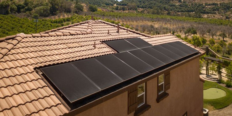
What is the Most Common Solar Panel
Currently, monocrystalline silicon panels are the most common, with conversion efficiencies as high as 15%-22%.
They are more durable than polycrystalline silicon, with a service life usually exceeding 25 years.
Due to high power generation per unit area and stable performance, although the price is slightly higher, they remain the mainstream preferred choice for residential and commercial rooftop installations.
Monocrystalline
High Purity
Currently, the mainstream monocrystalline silicon modules on the market all use 9N-grade virgin polycrystalline silicon material with a purity of 99.9999999% as raw material. This extremely high purity ensures perfect consistency in lattice arrangement.
Under the silicon wafer specifications of 182 mm (M10) and 210 mm (G12), the carrier mobility inside monocrystalline silicon is about 20% to 30% higher than that of polycrystalline silicon material.
This physical property directly results in a 15 percentage point reduction in the charge recombination rate, allowing the open-circuit voltage (Voc) of the cell to stabilize above 700 mV.
Currently, the mass production efficiency of P-type PERC monocrystalline cells has reached a bottleneck of 23.2%, while the average efficiency of new N-type TOPCon monocrystalline cells has directly crossed the 25.5% mark.
In the global photovoltaic module shipment structure, monocrystalline silicon, with this material purity advantage, has already occupied over 97% of the market share, completely replacing the polycrystalline technology that had a 40% market share 10 years ago.
Manufacturing Process
The core of monocrystalline silicon wafer production lies in the crystal pulling process, which requires continuous growth for 48 to 72 hours in a vacuum quartz crucible at 1425 to 1450 degrees Celsius.
To pull a monocrystalline silicon ingot weighing 300 kg to 500 kg, the pulling speed must be precisely controlled between 0.5 mm and 1.5 mm per minute to ensure 100% monocrystalline conversion rate.
In the slicing stage, current diamond wire cutting technology has reduced the wafer thickness from 170 microns to 130 microns or even 110 microns, reducing the silicon consumption per wafer by about 25%.
The surface of each silicon wafer creates a pyramid light-trapping structure with a depth of 2 to 4 microns through acid-base etching. This micron-level structure can capture over 98% of incident sunlight.
Concentrated in the ingot pulling stage, 20% to 30% of the electricity consumption during production is high, but this energy expenditure yields a rated power output of 50W to 80W more per square meter than ordinary panels.
High Efficiency
A typical 580W monocrystalline module consists of 144 half-cut cells, and its actual module efficiency is usually maintained between 22.4% and 22.8%.
Compared to the power density of 150 W per square meter 10 years ago, current monocrystalline technology has pushed this value above 225 W per square meter, an increase of 50% in power generation capacity per unit area.
Under medium light intensity of 800 W/㎡, the Fill Factor (FF) of monocrystalline panels can easily exceed 80%, meaning extremely low current loss.
Cells using 16BB (16 Busbars) or SMBB technology have a busbar resistance 10% to 15% lower than traditional 5BB, with a power gain of about 2W to 5W per cell.
This high efficiency directly reduces mounting material costs by 12% and DC cable procurement costs by 8%, because to achieve the same 10 kW installed capacity, a monocrystalline system uses about 6 to 8 fewer modules than old technologies.
Degradation Rates
The initial Light-Induced Degradation (LID) of monocrystalline silicon modules during the first year of operation has been controlled within 1.0%, and some N-type modules can even achieve below 0.5%.
During a warranty period of 25 to 30 years, the annual linear power degradation rate of this type of panel is only 0.4% to 0.55%, ensuring that 87.4% of the nominal power output remains at the end of the 30th year.
After passing 2000 hours of Damp Heat test (DH85), the power drop of high-quality monocrystalline modules is usually less than 2%, far better than the industry's 5% qualification standard.
The weather-resistant design of the backsheet can withstand 3,000 hours of UV radiation aging, and under a high system voltage of 1500 V, the anti-PID (Potential Induced Degradation) capability keeps power loss below 1%.
In contrast, the power of older polycrystalline silicon often falls below 80% after 20 years. The total power generation (kWh) of monocrystalline silicon over its entire life cycle is about 15% to 20% higher than that of polycrystalline silicon of the same specifications.
Cost and Pricing
Currently, the global wholesale price of monocrystalline silicon modules has dropped to between 0.10 USD and 0.12 USD per watt, a decrease of over 40% in the past 12 months.
For a residential system with a budget of 5000 USD, choosing monocrystalline modules usually accounts for 35% to 45% of the total investment.
Although the unit procurement price of monocrystalline panels is about 0.02 USD/watt higher than that of amorphous silicon or polycrystalline silicon, its Levelized Cost of Electricity (LCOE) is reduced by 12% to 18% due to high efficiency and long life.
In regions with abundant sunlight (such as annual utilization hours over 1500), the Return on Investment (ROI) period for monocrystalline systems has been shortened to 4.5 to 6 years.
Due to the high residual value of monocrystalline panels, even after 25 years of use, the recycling value of high-purity silicon material inside still accounts for 3% to 5% of the initial module cost, providing a more stable cash flow return for the entire life cycle of the power station.
Polycrystalline
Blue Pattern
The most intuitive feature of this type of panel is the irregular blue fragmented pattern on the surface. This visual effect stems from the thousands of small crystals with different orientations contained inside cells of 156.75 mm or 158.75 mm specifications.
Under standard sunshine intensity of 1,000 W/㎡, the sunlight reflectivity of polycrystalline silicon wafer surfaces is usually maintained between 5% and 10%, which is about 3% higher in reflection loss than alkaline-etched monocrystalline silicon.
The thickness standard for each polycrystalline cell is usually between 180 microns and 200 microns, about 20% thicker than N-type monocrystalline cells that pursue thinness.
Due to the presence of numerous grain boundaries, electrons encounter about 10% to 15% migration resistance when crossing these boundaries, resulting in Fill Factors generally in the range of 75% to 78%, making it difficult to break the industry high standard of 80%.
Cooling Casting
The manufacturing process of polycrystalline silicon mainly relies on a casting process, where 6N-grade industrial silicon material with 99.999% purity is placed in a quartz crucible and melted at temperatures of 1,200 to 1,300 degrees Celsius.
Compared to the 1450-degree Celsius high temperature required for monocrystalline pulling, this process saves about 25% to 30% in electrical energy consumption, with a single furnace production cycle typically shortened to 20 to 24 hours.
During the cooling crystallization process, through bottom-directional solidification technology, the silicon ingot grows upward at a rate of 1 to 2 centimeters per hour, forming a square silicon ingot with side lengths of about 60 to 80 centimeters.
Since it does not require 72 hours to grow a single crystal, the unit production cost of polycrystalline silicon is about 15% lower than that of monocrystalline silicon, which allowed it to occupy over 60% of the global market share before 2015.
Average Conversion
Currently, the average conversion efficiency of commercial polycrystalline silicon modules is generally between 15% and 17.5%, and the peak power output of a single 72-cell series module typically fluctuates between 320W and 350W.
In a laboratory environment at 25 degrees Celsius, the open-circuit voltage (Voc) of polycrystalline cells is generally stable around 630 mV, which is about 70 mV lower than the 700 mV benchmark of monocrystalline technology.
Its temperature coefficient is usually between -0.40%/℃ and -0.45%/℃, meaning that when the panel surface temperature rises to 65 degrees Celsius, its actual output power will drop by about 16% to 18% from the rated value.
Since the power density per unit area is only 150 W/㎡ to 170W/㎡, to achieve the same 10 kW installed capacity, a polycrystalline system needs to occupy about 65 square meters of installation space, which is about 15 square meters more than a high-efficiency monocrystalline system.
Very Low Budget
Polycrystalline modules are "price-sensitive" products in the current global wholesale market, with Factory on Board (FOB) prices usually maintained between 0.07 USD and 0.09 USD per watt, about 20% cheaper than mainstream monocrystalline modules.
For a 1MW large-scale ground-mounted power station project, choosing polycrystalline modules can save about 20,000 to 30,000 USD in initial procurement payments.
Although the cost per watt is lower, the low module efficiency leads to a 12% increase in mounting structure installation and a 10% increase in the use of DC combiner boxes and 4mm² cables. These rising Balance of System (BOS) costs offset about 5% of the module price advantage.
In tropical regions with annual rainfall exceeding 1,000 mm, the Return on Investment (ROI) period for polycrystalline modules is usually set at 6.5 to 8 years, which is about 18 months slower than monocrystalline power stations.
Durable
The physical stability of polycrystalline silicon modules has been market-proven for over 30 years, and its first-year power degradation rate is typically controlled between 2% and 2.5%.
During a 25-year linear power warranty period, the annual natural degradation rate of this type of panel is about 0.7%, meaning that in the 20th year, its power generation can still remain above 80.7% of the initial rating.
The TPT composite backsheet used on the back of the module can withstand 15 kV DC voltage tests, ensuring that it operates for 1,000 hours in high-temperature environments of 85% relative humidity and 85 degrees Celsius without delamination.
Since the sensitivity of the internal crystal structure to micro-cracks is about 5% lower than that of monocrystalline silicon, the breakage probability of polycrystalline cells is more robust when facing extreme wind and snow load tests of 2400 Pa negative pressure and 5400 Pa positive pressure.
Thin-Film
A Very Thin Layer
The thickness of the photosensitive layer in thin-film solar cells is typically only between 1 micron and 10 microns, which is only 1/100 to 1/20 of the thickness of crystalline silicon cells.
Currently, cadmium telluride (CdTe) modules occupy about 90% of the thin-film market, and the conversion efficiency of their commercial modules is generally maintained between 17% and 19%.
Copper indium gallium selenide (CIGS) cells have reached a record photoelectric conversion efficiency of 23.35% in laboratory environments, but the efficiency of mass-produced modules typically fluctuates in the range of 14% to 16.5%.
Amorphous silicon (a-Si) thin film is even thinner, about only one micron, but its conversion efficiency of 6% to 9% limits its application in large-scale power stations.
This extremely thin structure means that only 0.5 to 1 gram of semiconductor material is required to produce each watt of thin-film cells, significantly reducing the unit consumption of rare metals.
Thin-film modules are typically produced using vacuum sputtering or vapor deposition processes, and the entire manufacturing flow can complete the transformation from base glass to finished module within 2 to 3 hours.
This integrated production method reduces the production energy consumption per watt by about 40% compared to monocrystalline silicon, and the carbon payback time is shortened to between 0.5 and 1 year.
Due to the absence of physical limitations of silicon wafers, thin-film cells can be deposited on various substrates such as stainless steel, plastic, or flexible polymers. This feature allows the weight per square meter to be controlled around 2.5 kg to 5 kg, a reduction of over 60% compared to traditional 12 kg/㎡ glass-back crystalline silicon modules.
Heat Resistant
Thin-film solar panels have excellent temperature coefficients, usually between -0.20%/℃ and -0.25%/℃, far better than the -0.35%/℃ benchmark of monocrystalline silicon modules.
This means that when the operating environment temperature rises from 25 degrees Celsius to 65 degrees Celsius, the power loss of thin-film modules is only 8% to 10%, while the power drop of crystalline silicon modules can be as high as 14% to 16%.
In arid desert regions with annual sunshine intensity exceeding 2000 kWh/㎡, this extremely low heat loss can increase annual power generation per unit capacity by about 5% to 8%.
Under peak sunlight of 1,000 W/㎡, the output performance of cadmium telluride modules is about 4 W to 7 W higher in measured power than silicon modules of the same specifications, directly improving the overall energy yield of the power station.
Weak Light Performance
Thin-film cells have an extremely broad response to the spectrum, especially in the short wavelength range of 400 nm to 600 nm (such as cloudy days or early morning), where they have extremely high absorption rates.
Cadmium telluride modules can still maintain over 95% of their rated conversion efficiency under low irradiance of 200 W/㎡, while crystalline silicon often only performs at 85% to 90% under the same conditions.
This characteristic extends the daily power generation time of thin-film systems by about 20 to 40 minutes compared to silicon systems.
In cases of partial shading, the linear cell structure of thin-film cells can reduce power loss to within 10%, unlike silicon modules where damage to a single cell can lead to over 20% power drop in the entire string.
Flexible and Bendable
The bending radius of flexible CIGS thin-film modules can be reduced to 15 to 30 centimeters, allowing them to perfectly fit curved roofs or building facades with a radius of over 0.5 meters.
These modules are encapsulated with a 1.5 mm thick polymer, providing impact resistance sufficient to withstand the collision of 25 mm diameter objects moving at 23 m/s.
Under a wind pressure load of 2400 Pa, the probability of micro-crack propagation in flexible thin films is almost 0, while the micro-crack growth rate of crystalline silicon cells under the same pressure is about 5% to 15%.
By eliminating aluminum alloy frames and 3.2 mm tempered glass, the installation load requirement for the entire system drops from 15 kg/㎡ to 3kg/㎡, providing 100% photovoltaic coverage feasibility for old buildings with load-bearing capacities below 10 kg/㎡.
Lifespan
High-quality cadmium telluride thin-film modules provide a 25-year linear power guarantee, ensuring that after 300 months of operation, their output power is still not lower than 83% to 85% of the initial value.
First-year Light-Induced Degradation (LID) is essentially 0, better than the 0.5% to 1% initial loss of monocrystalline silicon.
The internal electrodes use special anti-permeation encapsulation technology, passing 2000 hours of 85°C/85% Damp Heat tests, with leakage current controlled below 10 microamps.
Currently, the recycling rate of such used modules has reached over 90%, allowing for the extraction of 99.999% purity tellurium and cadmium materials for reuse.
After being immersed in 1.5 meters of water for 48 hours, the insulation resistance of its IP68 junction box still remains above 400 megohms, ensuring 1500V system safety in extremely humid environments.
Pricing and Costs
In BIPV (Building Integrated Photovoltaic) projects, the installation cost of thin-film modules is typically between 1.5 USD and 2.5 USD per watt, depending on customized size specifications.
Although its wholesale module price per watt is about 0.30 USD to 0.45 USD, higher than the 0.12 USD of mainstream monocrystalline silicon, its Levelized Cost of Electricity (LCOE) advantage is clear in specific scenarios.
For example, in tropical regions with an annual average temperature above 30 degrees Celsius, the total 20-year power generation of a thin-film power station can be about 10% higher than that of a silicon power station of the same power, allowing its actual Return on Investment (ROI) to maintain a healthy level of 8% to 12%.
For commercial rooftop projects over 50 kW, choosing thin-film panels can reduce roof reinforcement costs by about 15% and labor handling time costs by 20%.