What is the Difference Between Photovoltaic Cell and Solar Cell
A photovoltaic cell directly converts sunlight to electricity via the photovoltaic effect, with single-crystal silicon reaching 26.8% lab efficiency (NREL 2023) and 22–25% in mass production.
A solar cell broadly includes thermal types (e.g., parabolic troughs) that first concentrate heat, achieving 15–20% total efficiency after converting heat to power (IEA 2022).
The key difference lies in the energy path: photovoltaic is direct light-to-electricity, while solar may involve intermediate heat steps.
Common Types
In 2023, monocrystalline silicon modules accounted for 92% of the global new photovoltaic installations, polycrystalline silicon accounted for 7%, and thin-film accounted for 1% (NREL); in the field of solar thermal power generation, parabolic trough systems accounted for 68% of the global installed capacity (2022 IEA).
The difference between the two types stems from the energy conversion path: photovoltaics generate electricity directly, while solar thermal first concentrates heat and then converts it.
Crystalline Silicon Types
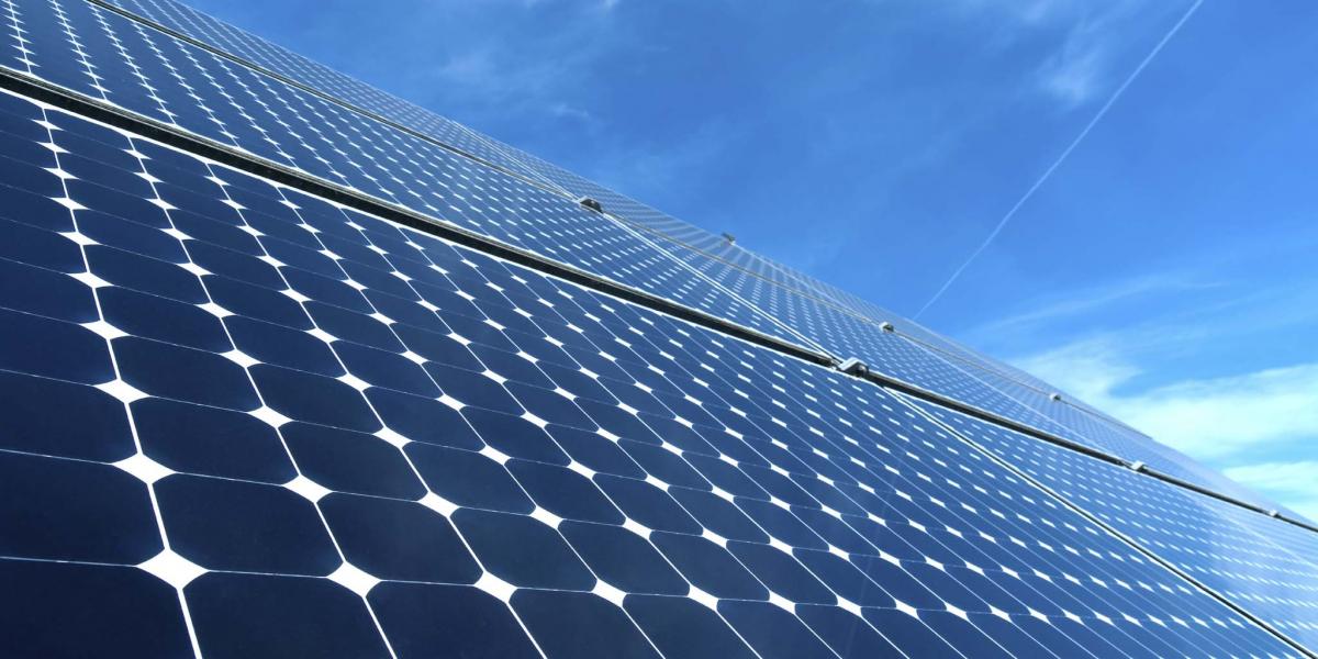
Crystalline silicon is the mainstream type of photovoltaic cell, divided into monocrystalline silicon and polycrystalline silicon.
Monocrystalline silicon is pulled from a single silicon crystal, with a highly ordered lattice and low electron migration resistance. Lab efficiency reaches 26.8% (2023 NREL), and mass-produced module efficiency is 22 to 25%. In 2023, its share in the global photovoltaic market exceeded 90%;
Polycrystalline silicon is spliced from multiple crystal grains, where grain boundaries slightly increase electron scattering. Mass production efficiency is 19 to 22%, with costs 15 to 20% lower than monocrystalline silicon. In the same year, its global module share was 7% (PV-Tech).
Both types use p-n junctions to separate photo-generated carriers. Monocrystalline silicon is more suitable for high-irradiation areas due to its high purity, while polycrystalline silicon has a cost-performance advantage on distributed rooftops. Together, crystalline silicon contributes more than 85% of global photovoltaic power generation (CPIA 2023).
Thin Film Categories
Thin-film photovoltaic cells generate electricity by absorbing light with ultra-thin semiconductor layers, commonly including amorphous silicon, cadmium telluride, and copper indium gallium selenide.
Amorphous silicon is only one micron thick and has excellent low-light response but an efficiency of 6 to 8%, and is prone to light-induced degradation; the mass production efficiency of cadmium telluride is 22.1% (First Solar 2023), and its flexible substrate can fit curved surfaces. In 2023, the global thin-film module market share was 1% (WoodMac);
Copper indium gallium selenide has an efficiency of 18 to 22% and good stability.
Thin-film material usage is only 1% of that of crystalline silicon, making it suitable for lightweight scenarios such as building-integrated photovoltaics, but the first-year degradation rate is 1 to 3%, and long-term efficiency maintenance is slightly inferior to crystalline silicon. It is currently mainly used in small off-grid or special-shaped projects.
Solar Thermal Branches
Solar cells broadly include solar thermal types, divided into parabolic trough, tower, and dish types. Parabolic troughs use parabolic mirrors to concentrate light and heat thermal oil in tubes to drive steam turbines. Global installed capacity accounts for 68% of solar thermal, with heat storage duration usually being 6 to 8 hours;
The tower type uses heliostats to reflect sunlight to a central receiver, with a concentration ratio exceeding 1000 times. The Dunhuang 100 MW project uses molten salt as a heat storage medium, achieving 12 hours of continuous power generation;
The dish type uses a rotating paraboloid to concentrate light, with a maximum efficiency of about 31% (NASA test), but the single-unit capacity is small and has not been scaled up.
In 2023, photovoltaics accounted for 89% of global solar investment, while solar thermal accounted for 11% (BNEF). Solar thermal types focus on heat storage and peak shaving, forming a complement to rather than a replacement for photovoltaics.
Conversion Efficiency
2023 NREL data shows that lab efficiency of monocrystalline silicon photovoltaic cells reached 26.8%, and mass-produced module efficiency is 22 to 25%; the total power generation efficiency of parabolic troughs in solar thermal systems after concentration is 15 to 20% (IEA 2022).
PV Efficiency
The lab efficiency of monocrystalline silicon photovoltaic cells reached 26.8% in 2023 (NREL). Efficiency of mass-produced modules dropped to 22 to 25% due to process losses. In 2023, monocrystalline silicon accounted for 92% of global new photovoltaic installations (PV-Tech);
Polycrystalline silicon cells are spliced from multiple crystal grains, where grain boundaries increase electron scattering. Mass production efficiency is 19 to 22%, with costs 15 to 20% lower than monocrystalline silicon. In the same year, the global module share was 7%.
Both types work based on p-n junctions. Monocrystalline silicon is better suited for high-irradiation areas due to its complete lattice, while polycrystalline silicon excels on distributed rooftops due to its cost-performance ratio.
Together, crystalline silicon contributes more than 85% of global photovoltaic power generation (CPIA 2023), with efficiency data directly linked to actual power output.
Solar Thermal Efficiency
The conversion efficiency of solar thermal cells requires calculating the total performance of concentrated heat collection and combined heat and power.
Parabolic trough systems use parabolic mirrors to concentrate light and heat thermal oil. The efficiency of the heat absorption stage is 55 to 60%, and the total power generation efficiency after driving the steam turbine is 15 to 20% (IEA 2022), with a heat storage duration of 6 to 8 hours;
The tower system uses heliostats to reflect sunlight to a central receiver, with a concentration ratio exceeding 1000 times. The molten salt heat storage of the Dunhuang 100 MW project makes the receiver efficiency reach 70 to 75%, with a total efficiency of 18 to 22%.
The dish system uses a rotating paraboloid to concentrate light, with a maximum efficiency of about 31% (NASA test). However, the single-unit capacity is small and has not been scaled up. Solar thermal efficiency is limited by heat transfer loss and heat storage media, forming a path divergence from direct photovoltaic conversion.
Efficiency Differences
Photovoltaic cell efficiency is constrained by material bandgap and carrier recombination rates. The theoretical limit for a single junction is the Shockley-Queisser limit of 33.7% (NREL). In 2023, the lab efficiency of perovskite tandem cells exceeded 32%;
Solar thermal systems require multiple steps including concentration, heat transfer, heat storage, and power generation. The cumulative losses at each step result in lower actual efficiency. Although dish solar thermal reaches 31%, it is difficult to promote.
In 2023, photovoltaics accounted for 89% of global solar investment (BNEF), while solar thermal accounted for 11%. The average efficiency of photovoltaics is 20 to 22%, and solar thermal is 15 to 18% on average.
Application Scenarios
In 2023, ground-mounted power stations accounted for 60% of global new photovoltaic installations, while distributed accounted for 40% (PV-Tech). In solar thermal power generation, the heat storage system configuration rate was 80% (IEA 2022). Due to different energy forms, scenarios have diverged from centralized grid connection to flexible peak shaving, with data density reflecting actual application preferences.
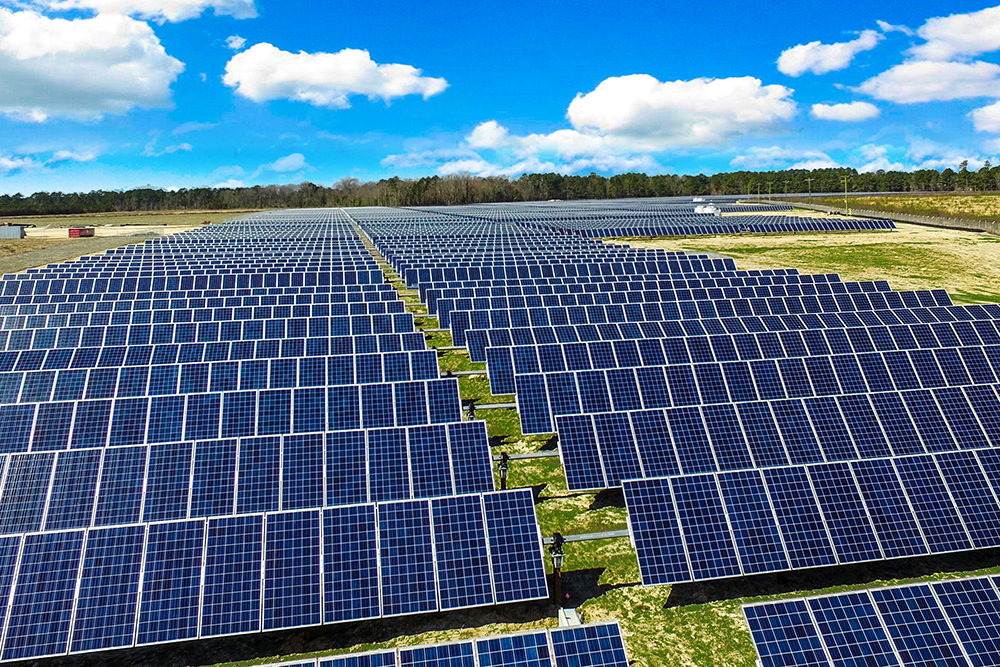
PV Ground-mounted Power Stations
Ground-mounted photovoltaic power stations rely on large areas of land to install modules centrally, mainly using monocrystalline silicon to pursue large-scale power generation and grid connection. In 2023, the average single-unit capacity of global ground-mounted power stations was 500 megawatts (NREL).
The mass production efficiency of monocrystalline silicon modules at 22 to 25% supports the implementation of projects with annual power generation exceeding 1 terawatt-hour, such as a 500-megawatt power station in Qinghai that meets the annual power demand of 800,000 households.
These scenarios choose high-irradiation deserts or Gobi areas. Module tilt is optimized according to latitude, and the support structure is designed for a wind load speed of 35 meters per second. The inverter efficiency is above 98.5%.
In 2023, ground-mounted photovoltaics accounted for 60% of global new photovoltaic installations, becoming an important supplement to the grid's base load power. Operation and maintenance mainly rely on drone inspections and string monitoring, with fault response time shortened to within 2 hours.
PV Distributed Scenarios
Distributed photovoltaics focus on rooftops, industrial and commercial plants, and agriculture-photovoltaic complementary projects, accounting for 40% of global new photovoltaic installations in 2023. Residential rooftops often use polycrystalline silicon modules with an efficiency of 19 to 22% to adapt to low-load roofs, while industrial and commercial rooftops choose monocrystalline silicon with 22 to 25% efficiency to increase output per unit area.
In agriculture-photovoltaic complementary projects, shade-tolerant crops are planted under the brackets, increasing land utilization by 30% compared to pure agriculture (CPIA 2023). For example, a 20-megawatt project in Shandong generates 24 million kilowatt-hours annually while producing 800 tons of mushrooms.
The scenario is characterized by local consumption and feeding surplus electricity into the grid. Inverters integrate anti-backflow functions, with a voltage fluctuation tolerance of ±10%. In 2023, industrial and commercial installations accounted for 55% of distributed photovoltaics, and residential accounted for 45%, becoming micro-units of urban energy transformation.
Solar Thermal Peak Shaving Applications
The core of solar thermal cell scenarios is heat storage and peak shaving, using concentrated heat collection and storage to compensate for the intermittency of photovoltaics. In 2023, the average heat storage duration of global solar thermal power plants was 8 hours (IEA). The molten salt heat storage of the Dunhuang 100-megawatt tower project reaches 12 hours, with an annual peak-shaving power of 300 million kilowatt-hours.
Scenarios are mostly selected in areas with strong sunlight and large grid peak-valley differences. For example, a 50-megawatt dish solar thermal plant in Spain works with photovoltaics, with power generation accounting for 15 to 20% during summer midday (BNEF 2023), and releasing stored heat to supplement the evening peak in winter.
The system includes a heliostat field, an absorption tower, and heat storage tanks. The mirror field tracking accuracy is 0.1 degrees, the receiver surface temperature is 565 degrees Celsius, and the steam turbine inlet steam parameters are 535 degrees Celsius and 13 MPa. In 2023, the growth rate of solar thermal installations in resource-rich areas such as Saudi Arabia and Chile was 12%, making it a stabilizer for grids with a high proportion of renewable energy.