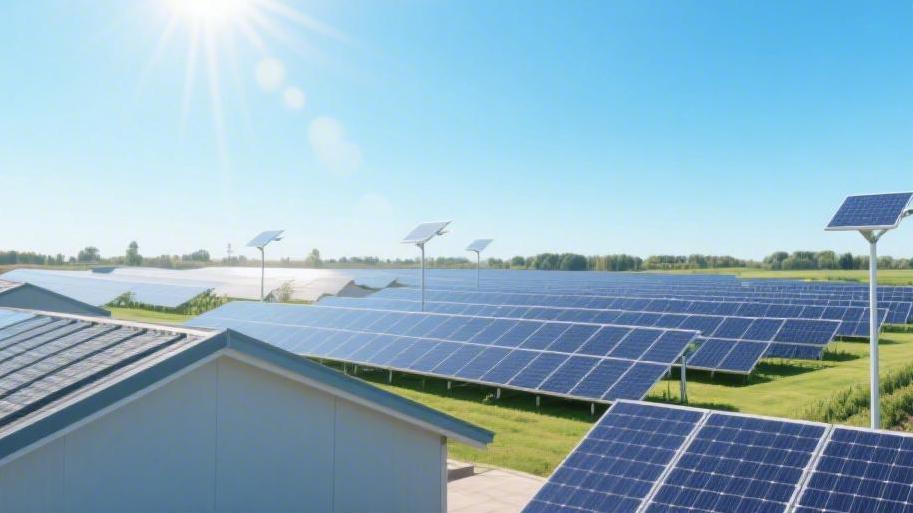
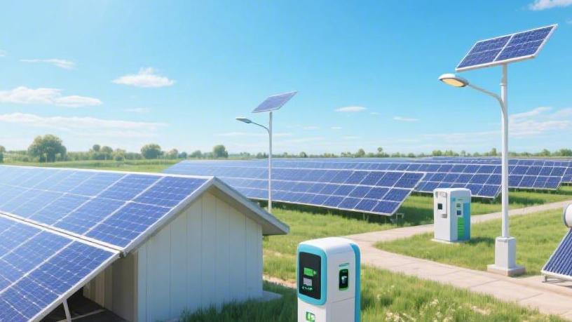
What are the Most Common Types of Solar Energy in 2026
In 2026, the most common type will be N-type TOPCon photovoltaic cells, with an expected market share of over 70%.
During manufacturing, by doping the silicon wafer with phosphorus and using double-sided glass encapsulation to absorb back-reflected light, its photoelectric conversion efficiency can be stabilized at over 26%, significantly improving actual power generation revenue.
TOPCon/HJT
In 2026, N-type cells have completely replaced P-type PERC technology in the market. TOPCon and HJT dominate the mass production conversion efficiency range of 25% to 26.5%. Standard M10 size silicon wafers with a side length of 182 mm can output an absolute power of 8.5 watts to 9.2 watts per single cell area. The average mass production efficiency of TOPCon has reached 25.8%, mainly relying on an ultra-thin silicon oxide tunneling layer with a thickness of only 1.5 to 2.0 nanometers.
HJT relies on an intrinsic amorphous silicon passivation layer to maintain the open-circuit voltage above 750 millivolts, pushing mass production efficiency to 26.2%. The silicon wafer thickness for both technologies has been significantly compressed. The standard wafer thickness for TOPCon is 130 micrometers, while HJT wafers have been thinned down to 110 micrometers. The breakage rate on the production line is strictly controlled between 0.8% and 1.2%. At the module end, standard packaging of the 72-cell layout is adopted, with external dimensions of 2,278 mm by 1,134 mm. The entire panel weighs 27.5 kilograms, and the output power is rated in the range of 610 watts to 630 watts.
The temperature coefficient of TOPCon is negative 0.29% per degree Celsius, while HJT has even better temperature performance, reaching negative 0.24% per degree Celsius. In an actual operating environment of 45°C, the power generation per watt of HJT modules is 3.5% to 4.2% higher than that of the older generation P-type panels.
Silver Paste Ledger
The metallization process consumes a large amount of non-silicon costs. The average consumption of silver paste for the front and back of TOPCon is 10 to 12 milligrams per watt, with a purity reaching 95%. Restricted by its 200°C low-temperature process, HJT can only use low-temperature silver paste, and the consumption increases to 15 to 18 milligrams per watt. The average market price of low-temperature silver paste remains at $850 to $920 per kilogram, which is 15% to 20% more expensive than high-temperature silver paste.
Factories blend 30% to 40% copper powder into the silver paste, reducing the pure silver usage per watt by 4.5 to 5.5 milligrams. The production line speed of the screen printing process reaches 6,500 to 7,200 wafers per hour, and the squeegee pressure is precisely set at 45 to 55 Newtons. This ensures that the printed fine grid lines are 18 to 22 micrometers wide and 12 to 15 micrometers high, compressing the panel's shading loss to below 2.5%.
Testing Results
N-type silicon wafers do not contain boron-oxygen complexes, completely eliminating the Light Induced Degradation (LID) phenomenon. The promised first-year power drop for TOPCon modules is between 0.9% and 1.0%, and the subsequent 29-year linear annual degradation rate does not exceed 0.35% to 0.40% at most. In its 30th year of operation, the panel can still output 87.4% of its initial rated power. The data for HJT modules is even lower, with a first-year degradation of 0.8% and a linear annual degradation rate of 0.30% to 0.35%.
In the accelerated aging laboratory, panels are continuously baked in an environmental chamber at 85°C high temperature and 85% relative humidity for 3,000 hours, resulting in a final power loss of only 3.2% to 3.8%. Ultraviolet aging testing inputs an irradiation dose of 60 kilowatt-hours per square meter, with the degradation value stabilizing at 1.1% to 1.5%. Dynamic mechanical load testing applies alternating pressure of positive 1,000 Pascals and negative 1,000 Pascals for 1,000 cycles, and the incidence of micro-cracks in the internal cells is below 0.5%.
Light on the Back
Both types of panels possess extremely high bifacial power generation capabilities and can absorb a large amount of ground reflection albedo to increase total output:
l TOPCon's bifaciality ratio reaches the test range of 80% to 85%.
l Relying on a completely symmetrical cell structure, HJT boasts a bifaciality ratio as high as 90% to 95%.
l On commercial flat roofs painted with white reflective paint, where the surface albedo reaches 65%, HJT's backside power generation can bring 18% to 22% additional electricity to the system.
l On dry desert surfaces with an albedo of 35%, the power generation from the backside gain ranges between 9% and 12%.
l When the mounting bracket clearance height is set to 1.5 meters and the panel tilt angle is maintained at 30 degrees, the irradiation received on the back reaches its maximum, generating an additional 150 to 200 kilowatt-hours of electricity per installed kilowatt annually.
l The power station's Ground Coverage Ratio (GCR) is optimized between 35% and 40%, effectively balancing the shading of front and rear arrays with the highest output per unit of land. The annual radiation captured per square meter of horizontal plane reaches 2,100 kilowatt-hours.
Factory Construction Accounting
There is a huge difference in the initial capacity construction capital expenditure between the two technological routes. For a 1-gigawatt capacity TOPCon cell production line, the pure hardware equipment budget is $22 million to $25 million. Low-Pressure Chemical Vapor Deposition (LPCVD) tube furnaces used to deposit the polysilicon layer account for 35% of the total equipment procurement amount, and the throughput of a single machine is 10,000 to 12,000 wafers per hour. A 1-gigawatt capacity HJT cell production line requires an investment of $45 million to $50 million.
Plasma-Enhanced Chemical Vapor Deposition (PECVD) chamber cluster equipment consumes 55% of the fixed asset investment. The HJT production line process is extremely simplified, usually consisting of only 4 to 5 main processes, while TOPCon requires 9 to 11 processes. The HJT factory footprint saves 25% to 30% of space.
TOPCon's current non-silicon manufacturing cost is $0.035 to $0.040 per watt. HJT's non-silicon cost is relatively high, fluctuating between $0.045 and $0.052 per watt. The consumption of indium metal deposited on the Transparent Conductive Oxide (TCO) film is 1.5 to 2.0 milligrams per watt. The spot market price of high-purity indium fluctuates between $400 and $450 per kilogram, driving up the final factory price of the module per watt.
Tandem
Under standard test conditions (25°C, 1,000 W/m² irradiance, AM1.5G spectrum), full-size mass production of M10-sized 2-Terminal (2T) perovskite and heterojunction (HJT) tandem cells with an area of 274 square centimeters has reached an average photoelectric conversion efficiency range of 28.5% to 29.2%.
The highest open-circuit voltage for small-area (1 square centimeter) single cells measured in the laboratory broke through 1.95 volts. The short-circuit current density was maintained at 20.5 to 21.5 milliamperes per square centimeter, and the fill factor (FF) stabilized between 82% and 85%. In terms of physical structure, the 2-terminal tandem design connects two materials with completely different crystal structures in series.
The top layer is a wide-bandgap perovskite thin film with a thickness of only 400 to 600 nanometers. Its bandgap is precisely tuned to 1.67 to 1.75 electron volts, specifically responsible for absorbing high-energy visible light and ultraviolet light with wavelengths between 300 and 750 nanometers. The bottom silicon-based cell has a bandgap of 1.12 electron volts and is responsible for absorbing near-infrared light with wavelengths between 750 and 1200 nanometers.
Top-Bottom Matching
The current output of tandem devices is limited by whichever is smaller between the top cell and the bottom cell current. To meet stringent current matching requirements, the manufacturing process inserts a transparent recombination layer with a thickness of 15 to 20 nanometers between the two cell layers.
The recombination layer acts as a tunnel for electron and hole recombination. Its own light transmittance must be higher than 95% in the 800 to 1,000 nanometer wavelength band, and the contact resistivity is suppressed to 0.1 to 0.5 ohms per square centimeter. Light passes through the front high-transmittance anti-reflective glass with a thickness of 2.0 mm, penetrates the front silver grid lines that are 30 micrometers wide and 15 micrometers high, and enters the perovskite absorption layer.
The top cell absorbs about 48% of the solar spectrum energy, while the transmitted low-energy photons are captured by the underlying 110-micrometer thick N-type silicon wafer. A complete module containing 72 tandem cells reaches a standard output power of 650 watts to 680 watts, which is 40 to 60 watts higher in absolute power than single-junction modules of the same area.
In a standard module encapsulation with an area of 2.58 square meters, the overall weight of the perovskite-crystalline silicon tandem panel is 28.5 kilograms. The highest mass production efficiency at the module level reaches 26.8%, the short-circuit current reaches 13.5 to 14.2 amperes, and the maximum operating voltage is set at 48 to 52 volts. To support such high output, paired microinverters or string inverters must widen their Maximum Power Point Tracking (MPPT) operating voltage range by 15% to 20%. In flat-layout power stations covering the same land area, tandem modules can reduce land footprint per megawatt by 12% to 15%.
Coating Machinery
Upgrading from a single-junction silicon wafer production line to a tandem production line does not require starting over from scratch. The factory retains the amorphous silicon passivation layer and transparent conductive film deposition equipment at the bottom of the heterojunction cell, and only needs to add a set of perovskite coating and crystallization modules measuring 35 to 45 meters long at the end. The capital expenditure for this newly added section of equipment is approximately $12 million to $15 million per gigawatt.
Solution-processed slot-die coating is the mainstream process. The gap between the coating die head and the substrate is controlled at 50 to 150 micrometers, and the coating speed reaches 2.5 to 3.5 meters per minute. After the ink spreads on the silicon wafer surface, it undergoes a vacuum extraction and thermal annealing process. The annealing furnace temperature is set at 100 to 130°C for a duration of 10 to 15 minutes, prompting the precursor solution to grow high-quality perovskite crystals with grain sizes of 1 to 2 micrometers.
The thicknesses of the electron transport layer (fullerene C60) and the hole transport layer (carbazole derivatives or polymers) are each controlled at 20 to 30 nanometers, usually accomplished using Atomic Layer Deposition (ALD) or vacuum thermal evaporation processes. The tandem retrofitting increases the non-silicon manufacturing cost per watt by $0.025 to $0.035, but the enhancement in absolute output power of the single silicon wafer dilutes the long-term Levelized Cost of Energy (LCOE).
The yield rate of the slot-die coating process has climbed to the current 92.5%. The utilization rate of coating ink has reached 85% to 90%, reducing the emission of precursor waste liquid containing lead, iodine, and bromine modules. The environmental treatment cost for recycling each ton of scrapped solution is $450 to $550, accounting for less than 0.1% of the total manufacturing cost.
Real-World Testing
Ion migration and sensitivity to water and oxygen are natural attributes of perovskite materials. To solve the challenge of long-term operation, encapsulation processes have undergone radical changes. Tandem modules have abandoned traditional ethylene-vinyl acetate (EVA) encapsulant films, fully shifting to Polyolefin Elastomer (POE) which has a lower water permeability. The Water Vapor Transmission Rate (WVTR) of POE film is lower than 2 grams per square meter per day.
The perimeter of the panel is edge-sealed using Polyisobutylene (PIB) butyl rubber water-blocking tape with a width of 12 to 15 mm, reducing the lateral water vapor ingress rate to below 0.0001 grams per square meter per day. After continuous baking for 2,000 hours in the Double 85 damp heat test (85°C, 85% relative humidity), the power degradation data of the tandem modules stabilized in the range of 4.5% to 5.2%.
Results from combined light and heat aging tests show that the panel efficiency remains above 93% of its initial value. The quality assurance terms offered by leading manufacturers for commercialized tandem modules promise a first-year degradation of less than 1.5%, and an annual linear degradation not exceeding 0.45% for the subsequent 24 years. Real measurement data from outdoor power stations indicates that while this panel's annualized degradation in high-UV equatorial regions is 0.1% higher than that of ordinary crystalline silicon panels, its annualized power generation in high-latitude low-light regions sees a 5% to 7.5% boost.
Bifacial
In the commercial installation data for 2026, dual-glass bifacial photovoltaic modules have reached an 85% market share in large-scale global ground power stations. The standard structure fully adopts 2.0 mm thick semi-tempered glass on both the front and back, completely replacing the opaque polymer backsheets of the past. The total thickness of the entire glass sandwich is 4.0 mm, and a standard 72-cell bifacial panel measuring 2,278 mm by 1,134 mm has its total physical weight precisely controlled at 32.5 kg.
The rated output power of the front side of the panel reaches 620 watts, and the photoelectric conversion efficiency under standard test conditions (25°C, 1,000 W/m² irradiance) stabilizes at 23.8%. The high-transmittance glass on the back features a 92% light penetration rate. Paired with a grid-like white ceramic color glaze coating that reaches a 30% coverage rate, the secondary reflectance of internal light is increased by 4.5%.
Bifaciality is an important physical metric, representing the ratio of backside efficiency to frontside efficiency. The bifaciality of current P-type and N-type hybrid modules is strictly controlled between 80% and 85%. If the panel's bifaciality is rated at 80%, under the same extremely strong illumination of 1,000 W/m² received on the back, the back can independently output an absolute power of 496 watts.
In a real outdoor operating cycle, the backside primarily relies on absorbing scattered light reflected from the ground. Over a complete 12-month operating cycle, it can bring an additional 5% to 30% power generation gain to the entire system.
Looking at Reflection
The data for extra electricity generated on the back depends entirely on the albedo index of the surface directly beneath the panel. The higher the albedo, the more shortwave radiation can bounce upward into the back cells. The mounting ground clearance is another highly quantified variable. If the height from the bottom edge of the panel to the ground is less than 0.5 meters, the shadow cast by the array itself will block 60% of the effective reflected light.
Raising the minimum ground clearance to 1.5 meters will increase the irradiation received on the back by 12% to 15%. However, the steel consumption of matching mounting brackets will correspondingly increase by 8 kg to 10 kg per kilowatt, driving up the initial hardware procurement budget. The differences in measured data across various surface environments are extremely obvious:
l Newly fallen pure white snow: The surface albedo is as high as 80% to 90%, which can generate 25% to 30% extra electricity, lowering the project's Levelized Cost of Energy (LCOE) by $0.005 per kilowatt-hour.
l White-painted concrete: Albedo is in the 65% to 75% range, bringing an 18% to 22% power generation gain, highly suitable for flat-roof commercial factory warehouses.
l Dry light-colored sand: Albedo remains at 35% to 45%, with a power generation gain of 10% to 15%, which is standard data for centralized desert photovoltaic power stations.
l Green grass and vegetation: Albedo drops to 15% to 25%, with a power generation gain of only 6% to 9%, common in agrivoltaic project sites.
l Dark asphalt or black soil: Albedo is only 8% to 12%, and power generation gain is as low as 3% to 5%. Compared to sandy environments, the investment payback period will be extended by 0.8 years.
Tracking the Sun
Combining dual-glass panels with Single-Axis Tracker (SAT) mounts is the hardware configuration strategy for achieving the highest Internal Rate of Return (IRR) in 2026. Tracker motors drive the entire solar array to rotate from east to west following the sun based on astronomical algorithms, with the maximum rotation deflection angle set at plus or minus 60 degrees.
A standard 100-megawatt flat single-axis tracker power station requires the installation of 3,000 independent drive shafts. Each row of shafts is pulled by a 24-volt DC motor, and a single motor's daily electricity consumption is only 0.05 kilowatt-hours. To prevent the front rows from casting shadows on the back rows when the solar elevation angle is low, the installation pitch of the array is widened to 6.0 meters to 7.5 meters.
Under sunlight conditions at 40 degrees north latitude, the equivalent annual utilization hours of this electromechanical combination can reach 2,200 to 2,400 hours. Procuring tracking systems increases the Capital Expenditure (CAPEX) per watt by $0.025 to $0.035, but the 15% to 20% increase in total power generation can recover this premium cost within 3.5 to 4 years.
Hardware Configuration Parameters | Fixed-Tilt Mounts | Flat Single-Axis Trackers | Dual-Axis Trackers |
Initial Installation Budget ($/W) | 0.015 - 0.020 | 0.040 - 0.055 | 0.085 - 0.110 |
Backside System Gain Ratio | 7% - 10% | 12% - 18% | 15% - 22% |
Land Footprint (Acres/MW) | 3.5 - 4.2 | 4.8 - 5.5 | 6.5 - 8.0 |
Annualized Mechanical Failure Rate | 0.1% | 1.5% - 2.0% | 4.5% - 5.5% |
Annual O&M Cost ($/MW) | 4500 - 5000 | 7500 - 8500 | 12000 - 15000 |
How Hard is the Glass
The physical encapsulation structure of dual-glass bifacial panels fundamentally eliminates backsheet aging risks caused by ultraviolet radiation, high humidity environments, and severe temperature fluctuations. The 2.0 mm thick photovoltaic glass has a water vapor transmission rate close to 0 grams per square meter per day. This completely blocks the pathway for moisture ingress to chemically react with silver grid lines, minimizing the probability of Potential Induced Degradation (PID) occurring.
In the limit testing chamber for dynamic mechanical load, the panel needs to withstand alternating pressure at 3 to 5 cycles per minute, with cyclic compression of positive 1500 Pascals and negative 1500 Pascals proceeding continuously for 2000 times. After the test, the micro-crack rate of the internal silicon wafers is detected to be below 0.3%, and the absolute power loss is strictly controlled to within 1.5%.
Facing static loads, the front of the panel can withstand 5400 Pascals of heavy snow pressure, which is equivalent to evenly stacking 550 kilograms of heavy objects on a 2.58 square meter surface. The back has passed 2400 Pascals of wind uplift force certification, capable of resisting strong wind impacts of 130 kilometers per hour. Because glass replaces polymer, the module's overall heat capacity becomes larger. Under 800 W/m² illumination and 1 m/s wind speed, its actual operating temperature is 1.5 to 2.5°C lower than that of single-sided modules. Relying purely on this temperature drop can recover 0.4% to 0.7% of relative power loss.
The warranties offered by top-tier manufacturers for these products include a 15-year material and workmanship guarantee and a 30-year linear power guarantee, with a commitment that the annualized degradation rate from the 2nd to the 30th year will not exceed 0.4%.