Monocrystalline vs Polycrystalline Panels | Structure, Efficiency, Differences
Monocrystalline silicon cell efficiency is about 20–23%, polycrystalline is about 15–18%; the former has a lifespan of more than 25 years and occupies less space.
When selecting models according to roof area and budget, prioritize monocrystalline (high efficiency), if budget is limited, choose polycrystalline, and calculate per-watt cost (about £0.2–0.4/W).
Structure
How it is smelted
The manufacturing of monocrystalline silicon wafers mainly relies on high-purity electronic-grade polycrystalline silicon material purified by the Siemens process. These raw materials with purity as high as 99.9999999% are put into a quartz crucible and melted at high temperatures of 1420°C to 1450°C. Through the Czochralski method, a seed crystal with a rotation speed of 10 to 20 revolutions per minute is slowly pulled up vertically, with the pulling speed controlled at 1 to 3 millimeters per minute, finally forming a cylindrical monocrystalline silicon rod with a diameter of usually 200 mm or 300 mm and weighing 300 to 500 kilograms.
In contrast, the manufacturing of polycrystalline silicon adopts the casting method, pouring molten silicon liquid into a ceramic mold for directional solidification, with a cooling speed of about 20°C to 30°C per hour. This lower manufacturing energy efficiency makes the production energy consumption of polycrystalline silicon ingots about 25% to 30% lower than that of monocrystalline. During the monocrystalline pulling process, a strong magnetic field of more than 1.5 Tesla is needed to suppress the silicon liquid convection.
· The operating vacuum of the monocrystalline furnace needs to be maintained between 10 to 30 Torr.
· The ratio of silicon material input to the weight of the output silicon rod is usually maintained within 1.1:1.
· The unqualified rate of silicon wafer edges produced by polycrystalline casting is as high as 15% to 20%, while monocrystalline is lower than 5%.
· The electricity cost of manufacturing monocrystalline silicon wafers accounts for about 18% of the total cost.
What it looks like inside
On a microscopic scale, the atoms of monocrystalline silicon are arranged in a perfect diamond square array, with a lattice constant of 5.43 Å. This highly ordered structure reduces the resistance of electron flow to the minimum.
The average grain size of polycrystalline silicon is only a few millimeters to a few centimeters, and dangling bonds at the grain boundaries will capture a large number of electrons, leading to its minority carrier lifetime usually being only 10 to 50 microseconds, while the minority carrier lifetime of high-quality monocrystalline silicon can easily break through 1,000 microseconds or even reach more than 5,000 microseconds. The resistivity distribution of monocrystalline silicon is more uniform, with the fluctuation range usually controlled within plus or minus 10%, ensuring that the current conduction loss on large-size cell cells is extremely small.
· The bandgap width of monocrystalline silicon is fixed at 1.12 electron volts (eV) at room temperature.
· The electric field strength at the grain boundaries of polycrystalline silicon is about 40% weaker than that inside monocrystalline.
· There may be more than 500 tiny dislocations distributed per square centimeter of polycrystalline silicon wafer.
· The thermal conductivity of monocrystalline silicon is about 148 W/(m·K), which is conducive to heat dissipation of the cell under high current operation.
· The diffusion length of photo-generated electrons inside the monocrystalline can exceed 300 microns.
Numbers after cutting
Currently, mainstream monocrystalline silicon wafers have fully entered the diamond wire cutting era. The diamond wire diameter has shrunk from the previous 60 microns to 35 to 40 microns, and the number of silicon wafers produced per ton of silicon material has increased by about 15%. The 182mm specification (M10) monocrystalline silicon wafer area is 331.24 square centimeters, while the 210mm specification (G12) reaches 441 square centimeters. This trend toward large sizes directly reduces the resistance loss at module connections.
The thickness of silicon wafers has also rapidly thinned from 170 microns to 130 microns to 150 microns. Under the premise of maintaining mechanical strength, the silicon consumption per silicon wafer has decreased by about 12%. After monocrystalline silicon wafers undergo acid cleaning, thinning, and texturing treatment, this structure can reduce the reflectivity of incident light from 35% to below 10%, while polycrystalline silicon, due to disordered crystal orientations, usually maintains a reflectivity of 15% to 20% after texturing.
· The kerf loss during the monocrystalline diamond wire cutting process is about 55 microns.
· The single-piece weight of an 182 mm monocrystalline silicon wafer is between 45 grams and 52 grams.
· The breakage rate caused by thinning is usually controlled within 0.5% on automated production lines.
· The front light-receiving area of monocrystalline batteries is about 1.8% higher than that of polycrystalline batteries of the same size.
· The power of a single 210mm module is about 50 to 80 watts higher than that of an 182mm module.
Are there many bad spots
P-type monocrystalline silicon wafers may experience a power attenuation of 1.5% to 2% within the first 100 hours of operation due to the influence of boron-oxygen complexes, but after adopting gallium doping technology, the first-year attenuation can be reduced to below 0.5%. Polycrystalline silicon wafers, because they contain a large amount of metal impurities (such as iron, aluminum, copper ions, etc), the aggregation of these impurities at grain boundaries will trigger Potential Induced Degradation (PID).
Under extreme tests of 85°C high temperature and 85% humidity, its power loss may exceed 5% within 96 hours. The linear attenuation rate of monocrystalline modules is usually maintained within 0.45% per year over 25 years. By the 25th year, its output power can still reach more than 87.4% of the factory value, which is about 5 to 8 percentage points higher than that of polycrystalline modules.
· N-type monocrystalline modules have basically no light-induced degradation, and the first-year power retention rate can reach 99%.
· The iron impurity concentration inside polycrystalline silicon wafers is usually 2 orders of magnitude higher than that of monocrystalline.
· The anti-snail trail ability of monocrystalline modules is more than 30% stronger than that of polycrystalline.
· Under a mechanical load pressure of 5400 Pascals (Pa), the probability of hidden cracks in monocrystalline silicon wafers is 12% lower than that in polycrystalline.
· In a long-term operating environment, the inverter mismatch loss of monocrystalline systems is usually lower than 0.2%.
Performance after becoming hot
The performance of photovoltaic panels is significantly affected by temperature. The power temperature coefficient of monocrystalline modules is usually between -0.34%/°C to -0.38%/°C. When the summer ambient temperature reaches 35°C and the module backplane temperature rises to 65°C, the actual power output of monocrystalline panels drops by about 13.6%. In contrast, the temperature coefficient of polycrystalline modules is often as high as -0.41%/°C or more. Under the same high-temperature conditions, the power drop will exceed 16.4%.
In areas with high annual average temperatures, the cumulative annual power generation of monocrystalline systems will be 3% to 5% more than that of polycrystalline systems with the same installed capacity. In addition, the open-circuit voltage (Voc) of monocrystalline batteries is usually above 0.7 V, while polycrystalline is only about 0.64 V. This higher base voltage allows monocrystalline systems to start 15 to 20 minutes faster than polycrystalline in low-light environments such as early morning or evening.
· The temperature coefficient of monocrystalline N-type batteries can even reach an excellent level of -0.30%/°C.
· The operating temperature of monocrystalline modules is usually 25°C higher than the ambient temperature.
· Under low illumination, the spectral response range of monocrystalline modules is smoother between 400 nm and 1100 nm.
· The module operating current mismatch rate of monocrystalline systems is controlled within 1% year-round.
· The system efficiency (PR value) of monocrystalline systems in high-temperature environments is usually stable at above 80%.

Efficiency
How much electricity can be produced
Current monocrystalline N-type TOPCon modules have a mass-produced conversion efficiency stable between 22.8% to 24.5%. Each square meter of panel can produce 228W to 245W of electricity under 1,000W standard sunlight. In contrast, the mass production efficiency peak of polycrystalline silicon modules stays at only about 18.8%, with an output of about 188 W per square meter. This efficiency gap results in the monocrystalline system saving about 20% to 25% of land or roof area compared to the polycrystalline system under the same installation capacity.
Taking a large-scale project with an installed capacity of 1 MW (1,000 kW) as an example, using 24% efficiency monocrystalline modules requires only about 4,166 square meters of pure cell cell area, while using 18% efficiency polycrystalline modules requires 5,555 square meters.
· In the solar spectral response from wavelengths of 400 nanometers to 1100 nanometers, the photon collection efficiency of monocrystalline silicon in the long-wave band above 800 nanometers is 12% higher than that of polycrystalline.
· The fill factor (FF) of monocrystalline batteries is generally higher than 80%, reaching up to 83%, while the fill factor of polycrystalline batteries usually swings between 76% to 78%.
· The single-piece power of 210mm specification monocrystalline modules has crossed the 700W mark, while the power of polycrystalline modules of the same size specification can often only reach 520W to 550W.
Fear of high temperature or not
The characteristic of photovoltaic cell power decreasing as temperature rises is determined by the power temperature coefficient. When the ambient temperature rises from 25°C to 65°C (the actual temperature of the module surface often reaches this value), the power loss of monocrystalline panels is about 11.6% to 12.8%.
· When the module surface temperature reaches the limit test point of 85°C, monocrystalline modules can still maintain about 80% of the rated power output.
· The output power of polycrystalline modules at 85°C will drop significantly to about 73% of the rated value. The energy escape speed per unit temperature rise is about 30% faster than that of monocrystalline.
· In tropical areas where the average annual temperature exceeds 30°C, the annual power generation per watt of monocrystalline systems is usually 5% to 8% higher than that of polycrystalline systems. The temperature tolerance alone contributes about 3% of the revenue difference.
Weak light okay or not
Due to the single internal lattice of monocrystalline silicon, the obstacle to electron migration is extremely small, and its series resistance is usually lower than 0.3 ohms, while the parallel resistance is higher than 1000 ohms·per square centimeter. This makes the leakage current of monocrystalline batteries in weak light extremely low, enabling them to reach the starting voltage of the inverter 30 to 45 minutes earlier than polycrystalline. Because there are a large number of grain boundaries inside polycrystalline silicon, electrons are easily captured by impurities at the grain boundaries under low radiation, resulting in its weak-light conversion efficiency dropping by 10% to 15% compared to standard strong light, while the drop for monocrystalline is usually controlled within 5%.
· Under extremely weak light of 100 W/㎡, the relative efficiency retention rate of monocrystalline modules is above 95%, while polycrystalline modules often fall below 85%.
· The equivalent power generation hours of monocrystalline systems per year are usually 100 to 150 hours more than those of polycrystalline systems, which mainly benefits from the weak light contribution during sunrise and sunset stages.
· For areas that are cloudy year-round, the cumulative power generation revenue of monocrystalline panels is more than 18% higher than that of polycrystalline, far exceeding the book value difference of their nominal efficiency.
Becoming old fast or not
Under the 2026 technical standards, the first-year light-induced degradation (LID) of monocrystalline N-type modules can be almost ignored, generally controlled within 1.0%, and the annual attenuation rate for the following 29 years is only 0.4%. Because polycrystalline modules have a high content of boron-oxygen complexes inside the silicon wafer, the first-year light-induced degradation is usually between 2.0% and 2.5%, and due to the expansion of micro-cracks at grain boundaries under thermal stress, the annual linear attenuation rate is as high as 0.7%.
After 25 years of operation, monocrystalline modules can still maintain more than 87% of the initial power, while polycrystalline modules can often only maintain about 80%. This 7% efficiency difference directly corresponds to the loss of net profit in the later operation of the power station.
· The 25-year average power generation efficiency loss rate of monocrystalline modules is 10.6%, while the efficiency loss rate of polycrystalline modules in the same period is as high as 19.3%.
· In the Damp Heat (DH) test, the power attenuation of monocrystalline panels after being placed in an 85% humidity and 85°C environment for 1,000 hours is usually less than 2%.
· Polycrystalline panels, in the same damp-heat test, often see power attenuation breakthrough 3.5% or even higher because impurities at grain boundaries are prone to electrochemical reactions.
Electricity energy loss points
The bulk resistivity of monocrystalline silicon wafers can be precisely controlled between 0.5 and 1.5 ohm·cm, and the distribution is extremely uniform, with a standard deviation of less than 0.1. The bulk resistivity fluctuation range of polycrystalline silicon wafers is between 0.5 to 3.0 ohm·cm. This non-uniformity results in the probability of local hot spots generated during the current collection process being 2.5 times higher than that of monocrystalline.
Since the monocrystalline surface can be prepared with a perfect pyramid light-trapping structure through the alkali etching method, its surface reflectivity can be reduced to below 2%; the polycrystalline surface mainly relies on acid etching to prepare pit structures, and the reflectivity is usually maintained at 4% to 6%.
· The size of the textured pyramids on the monocrystalline surface is distributed between 2 microns and 5 microns, which can realize multiple reflections and absorption of photons, increasing the internal quantum efficiency (IQE) to over 98%.
· The light-trapping structure on the polycrystalline surface has a poor capture ability for near-infrared light greater than 900 nanometers, resulting in its internal quantum efficiency being about 7 percentage points lower than that of monocrystalline in the long-wave band.
· On the metalized electrode contact surface, the contact resistance of monocrystalline is usually 15% lower than that of polycrystalline. This reduces the Joule heat loss when current enters the solder ribbon from the silicon wafer, directly improving the absolute efficiency of the module by 0.2%.
Differences
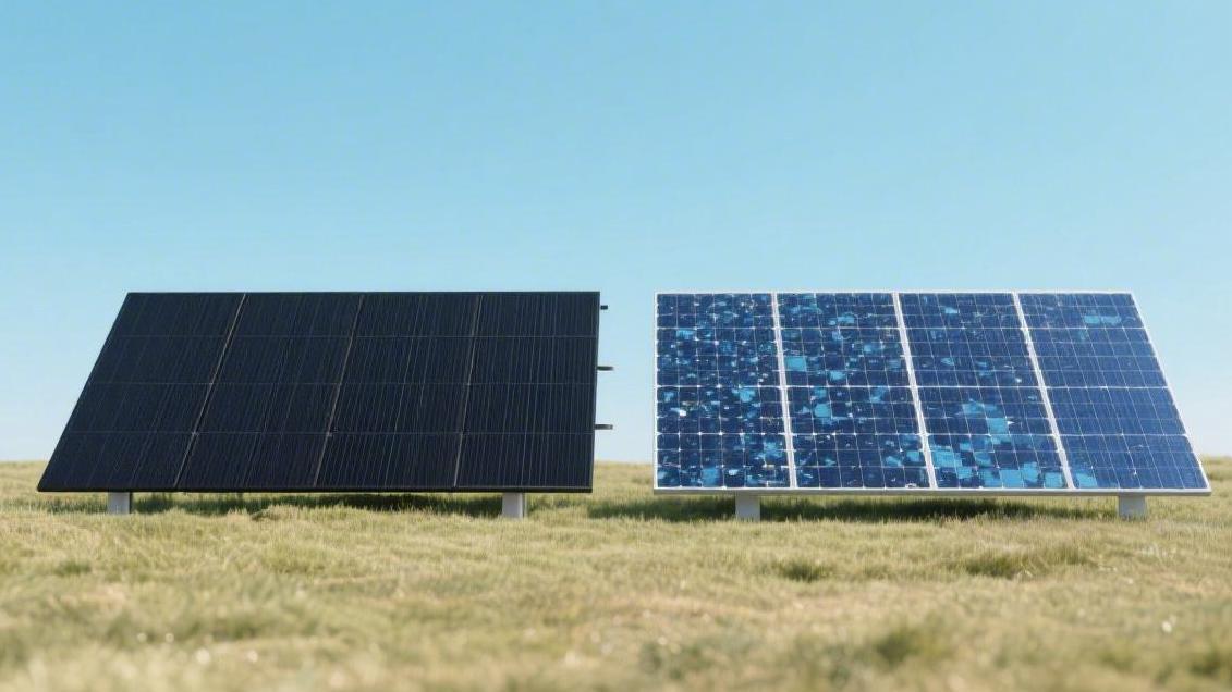
Color and shape
Since monocrystalline cell cells are sliced from complete silicon ingots, their molecular arrangement is highly consistent, appearing in a uniform deep black or pure black, and the four corners of the cell cells are usually cut off, forming a pseudo-square with rounded corner chamfers. Under standard lighting, the surface reflectivity of this black surface is only 1.5% to 2%, capable of capturing more photons with wavelengths between 400 nanometers and 1100 nanometers.
In contrast, polycrystalline cell cells are formed by cooling through a casting process, containing thousands of grains inside. The random orientation of these grains makes the surface appear as a deep blue texture similar to ice flowers or broken marble. Polycrystalline wafers are complete 90-degree right-angle squares. Due to the existence of grain boundaries, their surface reflectivity is usually as high as 4% to 6%. Even after coating treatment, their photon capture rate is still about 3% lower than that of monocrystalline.
When installing 60-cell modules of the same specification, the size of monocrystalline modules is usually 1640mm x 992mm. Since monocrystalline batteries have chamfered gaps of 1.5 mm to 2 mm, the effective light-receiving area utilization rate of the module surface is 92% to 94%.
How much money to pay
Market data for 2026 shows that the unit price per watt of monocrystalline modules is about 0.11 to 0.13 US dollars, while polycrystalline modules, due to the simple process chain, usually maintain a price of about 0.08 to 0.09 US dollars per watt, with an initial purchase cost about 25% lower. However, this unit price advantage quickly disappears when calculating the Balance of System (BOS) cost.
Due to the lower energy density of polycrystalline modules, to build a 1-megawatt photovoltaic power station, about 5500 modules are needed using polycrystalline panels, while only about 4,200 modules are needed using high-power monocrystalline panels. Monocrystalline systems can save 23% of bracket guide rails, 15% of DC combiner boxes, and about 20% of cable length, while manual installation man-hours also decrease by about 18% accordingly.
Taking a 10 kW residential project as an example, the total hardware expenditure for choosing monocrystalline modules is about 3500 US dollars, while polycrystalline is about 3000 US dollars. Although polycrystalline saves 500 US dollars of initial budget, because the annual power generation of monocrystalline systems is usually more than 15% higher than that of polycrystalline, this extra 500 US dollars of investment can usually be recovered through electricity bill income in the 3.5th year.
Land area size
Currently, the power density of mainstream monocrystalline panels has reached 210W/㎡ to 225W/㎡, while polycrystalline panels still stay at 170W/㎡ to 185W/㎡. On a small private villa roof with an area of only 50 square meters, monocrystalline modules can be arranged with a system capacity of 11 kW, while polycrystalline modules can barely squeeze out 8.5 kW in the same area. This 30% capacity gap directly determines the self-sufficiency rate of household electricity. In the case of adding energy storage batteries, the extra 10 to 15 kilowatt-hours of electricity generated by the monocrystalline system every day can cover the electricity demand for air conditioning for a whole night.
In large-scale ground power stations, land lease fees usually account for 5% to 8% of operating costs. Since the land area of monocrystalline systems is reduced by more than 20%, about 2000 to 3000 US dollars of land rent can be saved per megawatt each year. In addition, with the support of 210 mm large silicon wafer technology, the length of monocrystalline modules can reach 2.3 meters and the width 1.3 meters. Its internal circuit loss density is about 10% lower than that of polycrystalline.
Degradation speed
Due to its single lattice structure, monocrystalline silicon panels have very few internal impurities. Their first-year light-induced degradation (LID) is usually controlled within 1.5%, and some high-end N-type monocrystalline can even drop below 0.5%. Because there are a large number of grain boundaries inside polycrystalline silicon, these interfaces are gathering places for impurities and defects.
Under the action of long-term ultraviolet radiation and thermal cycling, impurities will undergo complex physical reactions, resulting in the first-year attenuation often reaching 2.5% to 3%. In subsequent operating years, the annual attenuation rate of monocrystalline is 0.4% to 0.5%, while polycrystalline fluctuates between 0.7% to 0.8%.
By the 20th year of operation, the actual output power of monocrystalline modules can usually still be maintained at 88% to 91% of the nominal power, while polycrystalline modules have often already fallen below the 82% warranty red line. This difference in attenuation speed means that in the later stage of power station operation (years 15 to 25), the annual power generation revenue of the monocrystalline system will steadily exceed that of the polycrystalline system by about 8% to 12%.
Fear of heat or not
For every 1°C increase in ambient temperature, the output power of monocrystalline batteries decreases by about 0.35%, while the decrease for polycrystalline batteries is as high as 0.42% to 0.45%. Under typical working conditions where the summer ambient temperature is 35°C and the panel surface temperature reaches 65°C, the power loss of monocrystalline panels is about 14%, while the power loss of polycrystalline panels will rush towards 18%. This 4% power gap will be amplified during the peak power generation period from 12:00 pm to 2:00 pm, resulting in the peak power generation capability of polycrystalline systems being far less stable than that of monocrystalline.
Experimental data shows that in tropical and subtropical regions where the annual average temperature exceeds 25°C, the annual utilization hours per watt of monocrystalline systems are about 120 hours higher than those of polycrystalline.
Carbon footprint much
The manufacturing of polycrystalline silicon adopts the casting method. Silicon material is melted in the furnace and then cooled. The electricity consumption of the whole process is about 15 to 20 kilowatt-hours per kilogram, and the Energy Payback Time (EPBT) is usually between 0.8 to 1.2 years. Monocrystalline silicon needs to use the Czochralski crystal pulling method, which must maintain a high temperature of 1425°C for a long time and drive the crystal to rotate.
The electricity consumption per kilogram is as high as 40 to 50 kilowatt-hours, and its energy payback period usually requires 1.2 to 1.5 years. Although monocrystalline consumes more electricity in the production stage, because its total power generation during its service life is more than 20% higher than that of polycrystalline, its average carbon emission density (grams of CO2/kWh) in its life cycle is actually about 5% to 8% lower than that of polycrystalline.
In the 2026 green finance audit, the carbon emission reduction contribution rate of monocrystalline systems is usually 15% higher than that of polycrystalline systems of the same power. For industrial and commercial customers pursuing carbon neutrality goals, despite the high initial investment in monocrystalline, the value of the carbon credits it generates is higher.