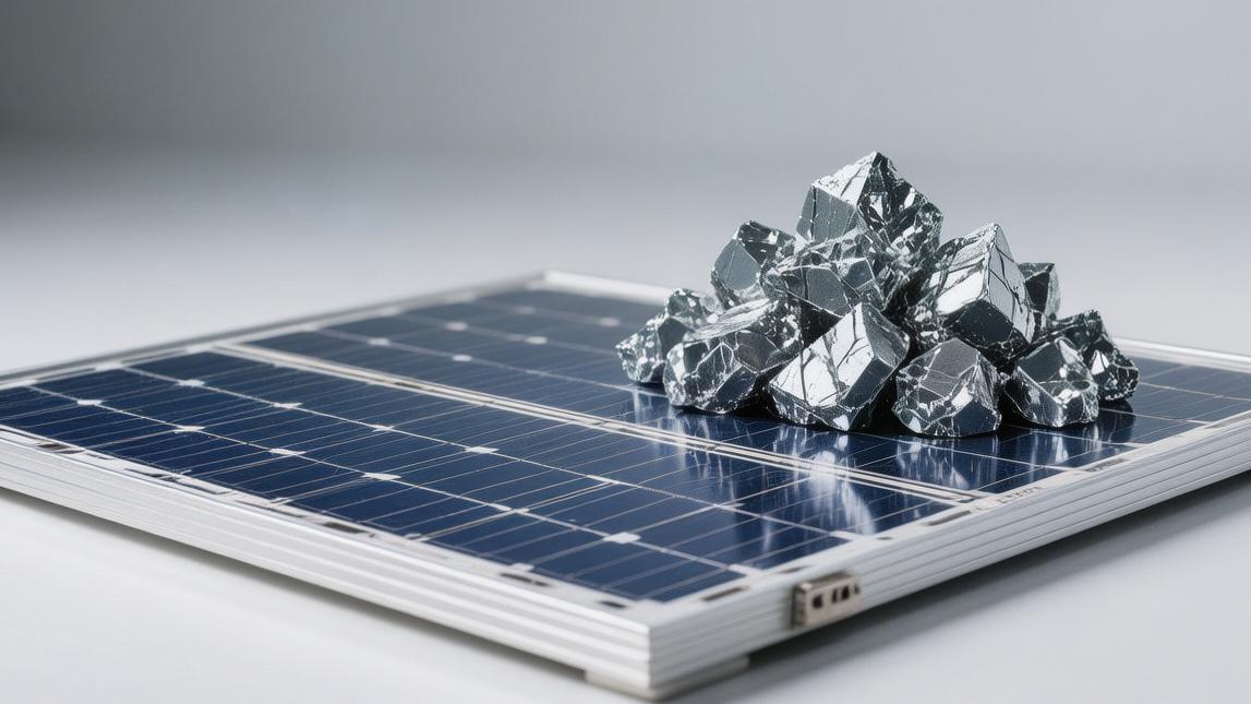
How much polysilicon is used in solar panels
With continuous progress in photovoltaic manufacturing processes, the current average polysilicon consumption of solar panels is approximately 2.5 to 3 grams per watt.
Taking a mainstream 400-watt standard residential solar panel as an example, a single panel requires about 1 to 1.2 kg of high-purity polysilicon.
Grams per Watt
Calculating Consumption
In 2015, the standard output power of polysilicon PV panels remained in the 250 W to 280 W range, with the silicon consumption per watt indicator as high as 4.8 g to 5.2 g.
With the popularization of monocrystalline silicon processes, the average photoelectric conversion efficiency of mass-produced P-type PERC cells reached 23.2% to 23.5% in 2023 globally, significantly reducing silicon consumption per watt to a statistical range of 2.25 g to 2.35 g.
Entering the N-type cell era, the mass-produced photoelectric conversion efficiency of TOPCon cells rose to 24.5% to 25.2%, and the standard output power at the module end increased from 550 W to over 580 W.
A single cell can output higher ampere current and volt voltage, and the corresponding silicon consumption per watt further dropped to the 2.05 g to 2.15 g range.
Heterojunction (HJT) cell open-circuit voltage surpassed 715 mV, and under standard test conditions (1,000 W/m² irradiance, 25 °C), the bifaciality rate reached 85% to 90%.
Its process allows the use of ultra-thin silicon wafers of 90 μm to 100 μm, and the silicon consumption per watt in theoretical design models dropped to an ultimate threshold of 1.8 g to 1.9 g.
Kerf Loss Rate
· Currently, the physical diameter of diamond wire used on mass production lines is controlled between 33 μm and 36 μm. When the wire diameter is reduced from 36 μm to 33 μm, the physical gap generated by each cut is correspondingly reduced by 3 μm. On a monocrystalline silicon square rod with a length of 1,000 mm, 100% full-load cutting can produce approximately 18 to 22 more standard silicon wafers with a thickness of 130 μm.
· At a slicing machine operating at a linear speed of 2,800 m/min to 3200 m/min, the physical breakage rate and micro-crack rate of silicon wafers are controlled within the 0.5% to 1.2% range. For every 1 percentage point increase in the actual yield rate of Grade A silicon wafers, the polysilicon raw material consumption distributed per watt of modules will decrease by about 0.025 g.
· Approximately 12% to 15% of high-purity silicon material is converted into micron-scale silicon powder suspension during the cutting process. Current centrifugal separation and filtration equipment can recover 75% of this waste at a purity standard of 98.5%, reintroducing it into a Czochralski monocrystalline furnace at temperatures as high as 1500 °C for secondary melting, increasing the effective raw material utilization rate from 85% to over 92%.
Looking at Dimensions
In physical size parameter calibration, mainstream silicon wafer specifications have fully upgraded from a side length of 156.75 mm (M2) to 182 mm (M10) and 210 mm (G12).
A 182 mm monocrystalline silicon wafer with an area of 33,127 mm², at a thickness specification of 130 μm, has a single-wafer physical weight between 10.5 g and 10.8 g.
At a 24.5% photoelectric conversion efficiency, a single monocrystalline silicon cell outputs 7.5 W to 7.8 W of electrical power under standard illumination, accurately locking the material consumption at 1.39 g/W at the single-wafer level.
When the size increases to the G12 specification with a side length of 210 mm, the physical area of the silicon wafer reaches 44,096 mm², and the corresponding weight increases to 14.2 g to 14.6 g.
The single-wafer output power simultaneously jumps to 10 W to 10.5 W, with silicon consumption per watt at the single-wafer level maintained within a small fluctuation range of 1.38 g to 1.42 g.
Precision control of the chamfer radius (usually 24.7 mm) during square-cutting of the front-end silicon ingot affects the weight of the peripheral residue.
For every 1 mm increase in chamfer error, the square block yield rate decreases by 0.3%, which in turn increases the comprehensive silicon consumption per watt of the entire process by 0.015 g.
Degradation Rate Ledger
The initial g/W indicator of materials only reflects the physical state at the factory. Over a service life of 25 to 30 years, the power degradation rate will change the lifetime g/kWh revenue model.
· N-type silicon wafers are doped with phosphorus rather than boron, eliminating the early light-induced degradation effect caused by boron-oxygen complexes. The first-year power degradation rate is strictly controlled within 1%, whereas traditional P-type cells have a first-year degradation rate between 2% and 2.5%. A 1% difference in power retention means that at the same silicon usage, the actual output power in the first year increases by about 5.5 W.
· During the operation cycle from year 2 to year 30, the annual average power degradation rate of single-glass backsheet modules is set at 0.55%. Bifacial double-glass modules rely on the sealing of 2.0 mm thick heat-strengthened glass to reduce water vapor transmission to below 0.01 g/(m²·day), lowering the linear degradation rate to 0.4%.
· A 550 W bifacial module containing 1.3 kg of polysilicon, in a latitude region with 1500 hours of sunlight per year, has a total power generation of about 23,000 kWh over 30 years. After 262,800 hours of natural environment operation, the 1300 g of silicon material can still maintain the electron transition frequency in the microscopic lattice at over 87.5% of the initial set value.
Temperature and Voltage
For every 1 °C increase in the working temperature of a solar cell, the carrier mobility within the polysilicon material undergoes microscopic physical changes, leading to a regular decrease in actual output power. This quantitative parameter is the temperature coefficient.
The power temperature coefficient of traditional P-type monocrystalline silicon modules is -0.34%/°C to -0.36%/°C.
When the outdoor ambient temperature reaches 40 °C, the actual physical temperature on the cell surface will soar to 65 °C. Compared to the standard test condition of 25 °C, the power output will suffer an absolute loss of 13.6% to 14.4%.
A panel originally rated at 550 W can only output about 470 W of actual power. In high-temperature working conditions, the instantaneous silicon consumption indicator passively climbs from the nominal 2.2 g/W to 2.76 g/W.
Modules manufactured with N-type silicon wafers with low oxygen and carbon content optimize the power temperature coefficient to the -0.29%/°C to -0.30%/°C range.
Under the same 65 °C high-temperature load pressure, the power output loss rate is reduced to 11.6% to 12%, with actual output power remaining above 486 W, and the high-temperature instantaneous silicon consumption maintained at 2.67 g/W.
Strictly controlling the oxygen concentration inside silicon atoms to below 10 ppma (parts per million atomic) and carbon concentration to below 1 ppma is the material parameter standard for maintaining low temperature coefficient physical characteristics.
Energy Footprint
How Much Electricity is Consumed
In the entire manufacturing process of polysilicon, purifying metallurgical-grade silicon with 98% purity to the 99.9999% photovoltaic-grade standard is an extremely energy-intensive industrial conversion process.
Currently, mainstream global capacity uses the modified Siemens process, growing silicon rods through chemical vapor deposition in a reduction furnace. For every 1 kg of high-purity polysilicon produced, the factory's electricity meter typically records 45 kWh to 55 kWh.
If the synthesis and rectification processes for trichlorosilane gas are added at the front end, the total electrical energy consumption will climb to the range of 60 kWh to 65 kWh per kg.
A new polysilicon purification plant with an annual capacity of 100,000 tons usually has a base electrical load as high as 800 MW to 1000 MW when operating at full capacity, equivalent to the full-load output power of a single unit in a medium-sized nuclear reactor.
To reduce this rigid electricity expenditure, granular silicon technology using the silane fluidized bed method has drastically cut the physical energy consumption of a single furnace reaction.
In a fluidized bed reactor, because the activation energy threshold for silane gas decomposition is low, the comprehensive electricity consumption per kg of polysilicon is significantly compressed to between 14 kWh and 18 kWh.
In the operating budget of large-scale polysilicon purification bases, electricity expenses steadily account for 35% to 42% of the total manufacturing cost. When regional industrial electricity prices fluctuate between $0.03/kWh and $0.05/kWh, the variance in pure electricity cost per kg of polysilicon reaches $1.2. This deviation is transmitted by percentage and affects the final budget for solar terminal panels.
High-Temperature Furnace
Polysilicon crystal growth depends entirely on the extreme thermodynamic environment control inside the reduction furnace.
The reduction furnace is a stainless steel pressure vessel with a volume of 20 m³ to 30 m³, where the internal air pressure is strictly set at a constant positive pressure of 0.5 MPa to 0.6 MPa.
Energized U-shaped silicon cores serve as heating elements, with temperatures soaring to between 1050 °C and 1150 °C within minutes.
Within this high-temperature range, trichlorosilane gas reacts with high-purity hydrogen, and the resulting silicon atoms deposit on the surface of the silicon core at a rate of 10 μm to 15 μm per hour.
The entire vapor deposition operation cycle lasts 72 to 96 hours, during which the temperature distribution inside the furnace must remain highly uniform, with the standard deviation of temperature deviation between any two points limited to ±5 °C.
Once temperature fluctuations exceed this limit, microscopic thermal stress defects occur in the polysilicon lattice, leading to a 15% to 20% increase in the probability of brittle fracture in the produced batches.
The bell jar outer wall of the reduction furnace needs to be forcibly cooled by pure water at a flow rate of 500 m³ to 800 m³ per hour, carrying away over 40% of the physical heat. Connecting this cooling water at 85 °C to 90 °C to a waste heat recovery exchanger can generate low-pressure steam with a flow rate of 30 to 40 tons per hour and a pressure of 0.3 MPa. This waste heat reuse improves the comprehensive energy efficiency of the entire plant by 12.5 percentage points at once.
Payback Period
A standard monocrystalline silicon PV module with a rated power of 400 W consumes about 400 kWh to 450 kWh of physical energy throughout the entire industrial chain process, from quartz sand mining, metallurgical silicon smelting, polysilicon purification, and wafer cutting to final panel lamination.
When this panel is installed in a temperate high-irradiance latitude region with an annual equivalent sunlight duration of 1600 hours, its actual annual power generation is approximately 510 kWh to 540 kWh.
Dividing the total energy consumption of module manufacturing by the actual annual power generation, the resulting energy payback period falls exactly between 0.8 and 1.1 years.
Over the panel's physical lifespan of 25 to 30 years, it spends more than 95% of its time in a net-zero carbon energy output state.
In the calculation model for lifetime carbon emission indicators, for every 1 kWh of electricity produced, the median greenhouse gas emissions allocated to the PV system are only 20 g to 25 g of CO₂ equivalent. This emission ratio is less than 3% of that of a traditional coal-fired power plant (average of 820 g CO₂ eq/kWh) and is below the lower limit of the emission standard deviation for combined cycle natural gas power plants.
The Circular Account
Inside the reduction furnace, only 10% to 15% of the trichlorosilane gas is converted into solid polysilicon at once, while over 85% of the remaining gas mixture, along with the reaction byproduct silicon tetrachloride, forms an exhaust gas stream at 300 °C that is discharged from the furnace.
The exhaust gas recovery system utilizes boiling point differences to liquefy and separate these gases in cryogenic condensation equipment at -60 °C.
Silicon tetrachloride liquid is then pumped at constant pressure into a cold hydrogenation reactor at temperatures above 1000 °C, where it is converted back into trichlorosilane by adding high-purity hydrogen and metallurgical silicon powder, with a single conversion rate controlled within the 22% to 26% process range.
Through a precision distillation tower group with up to 150 trays, impurity concentrations such as boron, phosphorus, and other metal elements are forcibly removed to below 10⁻¹⁰ (0.1 ppba).
Relying on this fully closed chlorine-hydrogen cycle network, for every 1 ton of high-purity polysilicon produced by the manufacturing plant, the absolute amount of external supplementary liquid chlorine consumption has been strictly compressed from the original 12 tons to the 0.2 ton to 0.3 ton range. The closed-loop recovery and utilization rate of high-purity chemical raw materials has reached over 98.5%, reducing the probability of heavy metal wastewater discharge to a theoretical minimum of below 0.01%.
Economic Perspective
Calculating the Detailed Accounts
When the market transaction price of polysilicon remains at a benchmark of $10/kg, the silicon material cost contained in each watt of the module is approximately $0.022 to $0.025.
For a medium-sized ground-mounted PV power plant with a total installed capacity of 50 megawatts (MW), the expenditure on silicon material alone reaches $1.1 million to $1.25 million.
If upstream silicon prices surge to a high of $30/kg due to supply-demand imbalance, the silicon cost per watt of the module will instantly jump to over $0.07.
In a PV project with a total investment budget of $0.25/W to $0.30/W, the proportion of silicon material cost will rapidly expand from less than 10% to 25% or even 30%.
This price transmission mechanism causes the Levelized Cost of Energy (LCOE) of downstream power plants to increase by $0.005 to $0.008 per kWh, directly extending the originally expected payback period from 7 to 8 years to more than 9 years.
Silicon Price (USD/kg) | Silicon Consumption per Watt (g/W) | Silicon Cost per Watt (USD/W) | Silicon Cost for 100MW Project (USD) | Proportion of Module Cost (Assuming $0.15/W) |
8.0 | 2.2 | 0.0176 | 1.76 Million | 11.7% |
15.0 | 2.2 | 0.0330 | 3.30 Million | 22.0% |
25.0 | 2.2 | 0.0550 | 5.50 Million | 36.7% |
40.0 | 2.2 | 0.0880 | 8.80 Million | 58.7% |
Investing Heavily
Building a high-purity polysilicon plant with an annual capacity of 100,000 tons typically involves capital expenditure (CAPEX) between $1 billion and $1.2 billion.
This is not just the cost of purchasing reduction furnaces and distillation towers, but also includes extremely expensive high-voltage substation construction and hazardous chemical treatment facilities.
Based on a 10-year depreciation cycle, the fixed cost allocated to each kilogram of polysilicon for equipment depreciation alone is as high as $1.0 to $1.2.
It typically takes 18 to 24 months for a plant to go from groundbreaking to truly producing qualified electronic-grade or photovoltaic-grade polysilicon, plus a capacity ramp-up period of 6 to 9 months.
This means investors must withstand the financial pressure of zero cash flow for as long as three years.
To maintain the factory's cash flow balance, the capacity utilization rate of the production line must remain above 80%.
Once the utilization rate falls below 50%, the unit manufacturing cost after allocation will soar by 40% to 50% due to the high proportion of fixed asset depreciation, leading to a cash loss for every kilogram produced.
Cash Flow
In the operating expense (OPEX) structure of polysilicon production, electricity and industrial silicon powder (metallurgical-grade silicon) are the two largest cash outflow items.
For factories using the modified Siemens process, electricity costs constantly account for 35% to 40% of the total cash cost.
If the local industrial electricity price is $0.04/kWh, the electricity cost to produce one kilogram of polysilicon (consuming 50 to 55 kWh) is $2.0 to $2.2.
Metallurgical silicon powder as a raw material typically has a consumption ratio between 1.08:1 and 1.10:1; that is, producing 1 kg of polysilicon requires about 1.1 kg of metallic silicon.
When the market price of metallic silicon is $2,000/ton (i.e., $2/kg), the raw material cost is approximately $2.2.
Including labor, maintenance, and auxiliary materials (such as hydrogen and liquid chlorine), the cash cost limit for top manufacturers can be controlled within $4.5/kg to $5.5/kg.
Once the market selling price drops below this cash cost line, the factory faces the risk of "hematopoietic function" failure and must use reserve funds to maintain electricity and wage payments.
Cost Item | Proportion Range | Specific Value Estimate (Based on $6.5/kg Total Cost) | Key Influencing Factors |
Electricity/Energy | 35% - 40% | $2.30 - $2.60 | Electricity price (Every $0.01/kWh fluctuation affects $0.55/kg) |
Metallic Silicon Raw Material | 30% - 35% | $1.95 - $2.30 | Mining and smelting supply and demand |
Depreciation/Amortization | 15% - 20% | $1.00 - $1.30 | Initial CAPEX and capacity utilization rate |
Labor/Maintenance | 10% - 12% | $0.65 - $0.80 | Automation degree |
Locking in Long-term Contracts
Since the expansion cycle of polysilicon capacity (2+ years) is much longer than the expansion cycle of downstream cell and module factories (6-9 months), there is a clear timing mismatch between the upstream and downstream of the supply chain.
To avoid the risk of sharp price fluctuations caused by this supply-demand asymmetry, leading global PV companies typically sign Long-Term Agreements (LTAs) for 3 to 5 years.
In these agreements, buyers prepay 10% to 15% of the total purchase amount as a deposit to lock in supply for the coming years.
Although specific monthly transaction prices still refer to the monthly weighted average price of the spot market, the long-term contract mechanism locks in the "volume," ensuring the factory still has "rice for the pot" during market shortages.
During the supply shortage period of 2021 to 2022, spot market prices for individual orders were once 15% to 20% higher than long-term contract prices.
This dual-track pricing system means that a small module factory without long-term contract protection may have raw material procurement costs $0.03 to $0.04 higher per watt than large competitors with long-term contracts, which is a fatal disadvantage in the PV manufacturing industry where profit margins are only 5% to 8%.
Competing for Yield
The price difference between monocrystalline recharging material (high-end material for N-type cells) and ordinary dense material (mainstream material for P-type cells) is usually between $1.5/kg and $2.5/kg.
For a factory with an annual capacity of 50,000 tons, if the output proportion of N-type material can be increased from 40% to 80%, the annual net profit can directly increase by $40 million to $50 million without any additional physical investment.
Conversely, if carbon content exceeds the standard due to operational errors, and the product is downgraded to cauliflower-like or coral-like material (low-grade material), the selling price will be directly discounted by 30% to 40%, even below the cash cost line.
Secondary materials can usually only be used for polysilicon casting or as filler materials, and their market demand is shrinking at a rate of 20% per year.
Therefore, controlling trace element impurities is not just a technical issue, but also the most core profit lever in various financial statements concerning factory survival.
For every 0.1 ppba reduction in metal impurity content, it is possible to strive for a 1% to 2% marginal premium in the final selling price.