What Innovations Are Changing Solar Cell Technology | Efficiency, Materials, Design
Perovskite tandem technology will make photoelectric conversion rate historically break through 30%.
On traditional silicon wafer coating ultra-thin new material, combining double-sided light transmission design, can additionally elevate 15% back surface power generation quantity, with lighter and thinner form large amplitude lower manufacturing cost.
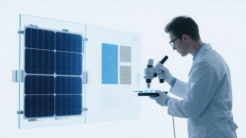
Efficiency
Where leaked electricity
Photons enter silicon wafer surface, not experienced chemical treatment's smooth crystalline silicon surface will reflect away about 30% of incident light rays. Factory assembly line on will on silicon wafer surface utilize alkaline liquid to corrode out height at 1 micrometer to 3 micrometers between's pyramid shape textured surface structure, and on surface layer cover thickness about 75 nanometers' silicon nitride anti-reflection coating film, through optical interference principle make surface reflectivity forcibly pressed low to 2% to 3% extremely low range.
Module front side's metal silver grid lines usually will block 3% to 5% of the light receiving area. Factory adopts multi-main grid welding process, making the original 5 strips width being 1 millimeter's main grid wires replaced into 16 strips to 20 strips width only 0.3 millimeters' cylindrical shape fine metal lines. Surface optical blocking rate lowered 1.5 percentage points, made front side silver paste's smear consumption quantity from single piece 110 milligrams reduced to 70 milligrams, whole piece cell's absolute conversion efficiency along with it increased 0.2% to 0.3%.
Under long-time light illumination, silicon wafer inside will happen boron-oxygen complex induced light-induced degradation (LID) phenomenon, P-type cell put into running's head 1,000 hours inside, efficiency absolute value will non-linearly drop 1.5% to 2.0%, change use phosphorus doped N-type silicon wafer after, first year light-induced degradation rate was strictly controlled in 0.5% extremely small variance range within.
Heat is making trouble
Photovoltaic panel at outdoor's actual running temperature does not locate at test standard stipulated's constant temperature of 25 degrees Celsius. Summer noon time, the ambient air temperature if reaches 35 degrees Celsius, absorbs a large amount of infrared thermal energy, and the module's actual measure temperature will usually soar to 65 degrees Celsius or even 70 degrees Celsius. Monocrystalline silicon module's power temperature coefficient median value locates at every degree Celsius -0.35% to -0.40%.
Working temperature every exceeds 25 degrees Celsius standard line 1 degree, total output power then will present a linear drop of about 0.35%. When the panel glass surface layer temperature reaches 65 degrees Celsius, the open circuit voltage will suddenly drop about 140 millivolts. This time, the whole piece module's actual electric energy output efficiency compared to the laboratory marked nameplate parameter drops 14.0%.
Factory adopts thinner's crystalline silicon slice (physical thickness from 170 micrometers gradually reduced to 130 micrometers) and matches thermal conductivity greater than 0.20 watts per meter Kelvin's polyolefin elastomer special encapsulation adhesive film, made module inside's lamination thermal resistance lowered about 18%, made panel actual working average temperature drop 2.5 to 3.0 degrees Celsius, can in period 90 days' summer running cycle inside recover about 1.2% power generation quantity loss.
Calculate account look at profit
Photoelectric conversion efficiency's even if 0.1%'s tiny elevation, on megawatt level's large scale ground power station financial report on all will produce a huge multiplier effect. According to the 2023 fourth quarter's global spot market average quoted price, monocrystalline silicon photovoltaic module's delivery price dropped to every watt 0.13 dollars to 0.15 dollars. In a covering area of 100 acres, the grid-connected installed total capacity is 50 megawatts' standard ground photovoltaic project inside. If the purchase module's average efficiency is elevated from 22.5% to 23.5% (absolute increase amplitude being 1.0 percentage points):
· Single piece physical area 2.58 square meters' standard photovoltaic module, its rated output power can increase from 550 watts to 575 watts, single piece power increase amplitude reaches 4.54%.
· In total, installed capacity load 50 megawatts, maintain not change's budget premise under, project needed's module physical purchase total quantity from 90900 pieces reduced to 86950 pieces, reduced 3950 pieces' mechanical carrying and installation working quantity.
· Accompanying physical installation quantity's reduction, underground piling area and matching's galvanized steel bracket weight can save about 120 tons, arrays between connection used's direct current side copper core cable length shrinks about 4.5 kilometers.
· Containing land lease, metal bracket, AC DC cable, manual installation fee in the inside's balance of system cost, the average every watt can save 0.012 dollars to 0.015 dollars.
· In photovoltaic system maintenance running's 25-year life cycle inside, according to annual average 1500 hours' effective equivalent sunshine time distribution statistics calculation, the overall levelized cost of energy will drop from every kilowatt-hour 0.045 dollars to 0.0415 dollars, project financial model's internal rate of return realizes about 0.6% to 0.8% quantitative growth.
Materials
Change formula
Silicon material towards photons' absorption coefficient relatively lower, requires silicon wafer's physical thickness must be maintained at 130 micrometers to 150 micrometers between then can intercept enough quantity's photons.
Research room cast sight towards having ABX3 crystal structure's new type semiconductor material. Among them, A is usually a methylammonium ion or formamidinium ion, B is a lead element, and X is an iodine or bromine element's halogen atom. A set of brand new chemical combinations made light absorption coefficient pulled high to every centimeter 10's 5th power, workers only need to spin coat a layer thickness of only 300 nanometers to 500 nanometers' light-absorbing thin film, then can absorb away 93% of the visible light wave band energy.
Thickness lowered to traditional silicon wafer's one fifth. Material ratio's fine tuning will produce huge physical parameter fluctuations, through changing iodine and bromine's mixing percentage, new thin film's band gap can be in the 1.2 electron volts to 2.3 electron volts' broad range, inside carry out continuous and precise adjustment.
Producing this layer micrometer-level light-absorbing thin film's solution coating process, only needs in a 100 degrees Celsius to 150 degrees Celsius low temperature oven environment inside heat roast 10 to 20 minutes then can complete crystallization, compared to purify monocrystalline silicon needed's 1450 degrees Celsius ultra high temperature melting furnace, manufacturing link's single watt energy consumption quantity dropped about 85%, factory production line's fixed asset investment fee is only one fifth of the same scale production capacity silicon-based factory.
Space style
Gallium arsenide belongs to the III-V group compound semiconductor, possesses 1.43 electron volts' extremely good energy band structure characteristic. When sunlight passes through a thickness of only 2 micrometers' gallium arsenide epitaxial layer, 99% of the effective photons can be captured and converted into electron-hole pairs, electrons in the material's mobility rate as high as every volt second 8,500 square centimeters, is common silicon material's 6 times.
In the laboratory's standard test model inside, the single junction cell's conversion efficiency peak value rushed to 29.1%. Facing above zero 120 degrees Celsius to below zero 150 degrees Celsius' extreme thermal cycle alternating environment, monocrystalline silicon module's open circuit voltage will happen violent fluctuation, gallium arsenide cell's power temperature coefficient is only every degree Celsius -0.08%, in high temperature load working condition, still can maintain extremely high voltage output stability. Construction costs extremely expensive, in a metal organic chemical vapor deposition reaction chamber inside grow high quality crystals, single square meter's materials and equipment amortized cost locates at 30,000 dollars to 50,000 dollars range.
In order to make every watt 100 dollars to 300 dollars' manufacturing cost cut down, engineers adopt epitaxial lift-off technology, use hydrofluoric acid solution to make the top part's few micrometers effective power generation thin film from the bottom part's thick heavy substrate, peel off down, same one expensive's base crystal wafer can cyclic reuse 20 to 50 times, make overall's single piece construction cost budget shrink 60% above.
Steam glass
Cadmium telluride is a band gap of 1.45 electron volts semiconductor, exactly matches the solar spectrum's energy distribution's most dense peak wave band. Assembly line on adopt vapor transport deposition equipment, on building glass surface evaporate coat on 2 micrometers to 3 micrometers thick's polycrystalline thin film. From a piece of white glass entering the production line at the start, experience vacuum coating, laser scribing, lamination encapsulation, to ultimately become a piece possessing power generation ability's complete panel, the whole production cycle's time was compressed to 3.5 hours within.
Because removed consume time's silicon ingot growing and physical cutting steps, according to life cycle assessment system, cadmium telluride panel every emits out 1 kilowatt-hour of electric energy that emitted's greenhouse gas is only 11 grams to 14 grams carbon dioxide equivalent, not reach monocrystalline silicon module 50 grams emission standard's one third.
New material in humid environment inside's anti-high temperature performance indicator extremely good, in environment temperature 75 degrees Celsius, relative humidity 85% double extreme pressure applied under, passed 2000 hours continuous exposure test, its conversion efficiency's degradation deviation rate maintains in extremely low's 3.5% range within, currently laboratory recorded's highest photoelectric conversion rate record stops at 22.1%, mass production commercial panel's average efficiency number reaches 19.0% to 19.5% between.
Design
Stack two layers
The top part's perovskite layer band gap was adjusted to 1.68 electron volts, specially responsible for capturing wavelengths at 300 nanometers to 750 nanometers between high energy blue-green light photons, making them convert into exceeding 1.15 volts' open circuit voltage.
Penetrate the top part of the thin film's wavelength at 750 nanometers to 1200 nanometers between infrared biased photons, then are by bottom part band gap being 1.12 electron volts' 130 micrometers thick crystalline silicon layer total number absorbed. Two layers materials series connection after, whole piece cell's test open circuit voltage number accumulated to 1.95 volts to 2.05 volts' range. Single junction silicon cell theoretical extreme value was stuck at 29.4%, double junction tandem architecture's theoretical physical efficiency upper limit was pushed high to 43.0%.
Laboratory produced out's 1 square centimeter test sample, in 1000 watts/square meter's standard light intensity under, photoelectric conversion efficiency peak value stably at 33.9%. Enter area being 274 square centimeters' large dimension mass production verification stage, calculated out's module average efficiency distributes at 28.5% to 29.0% between. According to every square centimeter, 15 milliamperes' short circuit current density calculate, in the 25-year expected life range, double junction design can make system total power generation quantity pull elevate 18% to 22%.
Back surface also absorbs light
The single-sided light-generating panel's back sheet is usually not a transparent fluorine-containing polymer thin film, changed into thickness being 2.0 millimeters' high light transmittance physical tempered glass, then constituted a double-sided double-glass structure.
When sunlight with a 35-degree angle illuminates the ground, snow fields' ground surface reflectivity is as high as 80%, white concrete's reflectivity is at 30%, and dry grass land's number hovers at 15% to 20%. Installed on leave ground clearance 1.5 meters metal bracket on's double-sided module, back surface silicon wafer can absorb from ground surface catapulted back coming's scattered photons.
Mainstream production line's P-type double-sided panel, its back surface bifaciality parameter (back surface efficiency and front surface efficiency's ratio) stably in the 70% to 75% variance range, N-type panel's back surface bifaciality then approaches 80% to 85%. In the equator nearby latitude 20 degrees region's sand land photovoltaic power station actual measure data indicates, double-sided design can let single piece output power be 550 watts' panel, at noon 12 o'clock's peak load time period additionally produce 45 watts to 55 watts' back part power increment.
In the whole year, 8,760 hours' running cycle inside, the whole set double-sided system's annual average actual power generation profit compared to the single-sided system increased 7.5% to 11.5%. Two pieces of glass let every square meter module's physical weight increase 4.5 kilograms, every watt's purchase budget slightly increased 0.005 dollars, calculated down internal rate of return number on the contrary climbed 0.4 percentage points.
Architecture classification | Front side optical blocking rate | Module area utilization rate | Peak output power increase amplitude | Production line every watt manufacturing cost | Full life cycle power generation gain | Expected power attenuation median value |
Conventional single-sided full piece | 4.5% - 5.0% | 93.5% | Baseline 0% | 0.12 dollars | Baseline 0% | Every year 0.55% |
Double-sided double-glass half piece | 3.0% - 3.5% | 94.0% | 8.5% - 12.0% | 0.13 dollars | 7.5% - 11.5% | Every year 0.45% |
High density shingles | 2.5% - 3.0% | 98.5% | 15.0% - 18.5% | 0.15 dollars | 10.0% - 14.0% | Every year, 0.40% |
Back contact no main grid | 0% | 99.5% | 22.0% - 25.5% | 0.22 dollars | 15.0% - 19.5% | Every year 0.35% |
Cut open stick tight
Physics law indicates, metal conductive wire inside's power thermal loss and current number value's square become direct proportion. Make side length 182 millimeters or 210 millimeters' standard square shape silicon wafer, use laser cutting machine one divided into two become half piece structure, single piece flow through's short circuit current instant from 13.5 amperes halved to 6.75 amperes. Internal current halved, module inside silver main grid line's resistance thermal loss doubled sudden drop, overall power output loss rate from original's 2.5% sharp reduce to 0.6% below.
In order to further elevate surface area's use density, the factory removed half-piece batteries between the originally retained 2 millimeters conventional physical spacing, adopt conductive adhesive to make adjacent cell pieces edge overlap 1.2 millimeters bonded together, and make into shingled module. A piece area being 2.58 square meters' standard encapsulated panel, inside can more stuff into 5% to 7% effective light-generating silicon material, make effective receive light area proportion from 93% climb to 98.5%.
In light intensity 500 watts/square meter to 1000 watts/square meter's dynamic fluctuation range within, shingled module's fill factor median value stably at 81.5% above, same dimension specification's panel, peak rated power number value increased 15 watts to 25 watts.
Make wire hide back face
Light receiving surface's optical blocking rate from 3.5% cleared to zero to 0%, panel front side realized 100%'s exposed light absorbing area. In order to prevent back-surface positive and negative electrodes from short-circuiting, the back surface needs to adopt ion implantation or high-temperature diffusion process, alternately produce out width at 150 micrometers to 250 micrometers between P-type and N-type doped regions.
Removed front side's metal contact recombination region, surface recombination speed rate large amplitude dropped, open circuit voltage parameter steadily crossed 740 millivolts' threshold, mass production batch's average conversion efficiency median value rushed to 24.5%. Complex's back surface mask and etching steps make single strip production line's process flow nodes from 9 increased to 14, production cycle time pulled long about 45 minutes.
High difficulty's manufacturing process made factory delivery price pushed high to every watt 0.22 dollars to 0.25 dollars' range. Expensive construction costs make it very hard to enter large-scale ground power station purchase lists, relying on zero blocking's appearance face value and every square meter exceeding 230 watts' high power density distribution. This kind of architecture in space-limited city villa roof installation market took down nearly 15% of the share occupation rate.