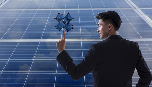
What are the advantages of perovskite solar cells over silicon solar cells
Perovskite cells hit 26% lab efficiency (vs silicon’s 23%), use low-energy solution printing (slashing costs 30%) and need 500nm thickness (95% less than silicon’s 200μm), enabling flexible, resource-light deployment.
Cheaper Manufacturing Process
The process begins with metallurgical-grade silicon, which must be purified in electric arc furnaces at temperatures exceeding 1900°C. This material is then converted into polysilicon and crystallized into large ingots, a process that requires maintaining temperatures above 1400°C for several days. These ingots are then sliced into wafers about 160-180 microns thick using diamond-wire saws, a wasteful step where approximately 40-50% of the high-purity silicon is lost as "kerf dust." The entire sequence, from raw quartz to a functional cell, can take over 72 hours and requires specialized facilities costing $1 billion or more to build.
The perovskite manufacturing pathway is fundamentally different, resembling roll-to-roll printing more than high-temperature semiconductor processing. This shift from a thermal-intensive batch process to a solution-based continuous one is the core of its cost advantage.
This ink can be deposited onto a substrate using techniques like slot-die coating or blade coating at temperatures predominantly below 150°C. Compared to the sustained 1400°C needed for silicon crystallization, this represents an order-of-magnitude reduction in energy consumption for heating, potentially slashing that portion of the energy bill by over 80%. The process is also remarkably fast; the liquid coating can be transformed into a high-quality, light-absorbing crystalline film in less than 60 seconds using simple heating or air flow. This contrasts sharply with the hours needed for silicon wafer doping and passivation. Furthermore, the material utilization efficiency is superior.
In advanced deposition methods, over 95% of the perovskite ink is applied directly onto the substrate, compared to the ~50% material loss from kerf during silicon wafering. The active layer itself is exceptionally thin—only 0.3 to 0.5 microns—meaning 500 times less material is needed by volume than a 180-micron thick silicon wafer to achieve the same light-absorption performance.A single silicon ingot grower can cost over 2 million ,and a single diamond−wire saw adds an other 1 million, with a full production line requiring many of these machines. A perovskite coating line, utilizing adapted equipment from the printing industry, is significantly less expensive.
A 2021 National Renewable Energy Laboratory (NREL) analysis estimated that the capital investment for a perovskite module production line could be approximately 70% lower than for a comparable silicon line. This lower CapEx, combined with faster processing times and higher material yield, directly translates to a lower cost per watt. While a mainstream silicon module cost has hovered around 0.20 to 0.25 per watt in recent years, perovskite manufacturing has a credible pathway to achieving costs below $0.15 per watt at scale, primarily driven by these fundamental advantages in process simplicity, material economy, and reduced energy intensity.
Less Material for Same Power
A standard silicon wafer needs to be about 160-180 microns thick—roughly the width of two human hairs—to absorb a sufficient amount of sunlight. This structural requirement is not just about light absorption; it's also because silicon is mechanically brittle and needs that thickness to be handled during manufacturing and installation without breaking. This results in a significant amount of material use per cell, and the sawing process to create these wafers from a solid ingot wastes nearly 50% of the high-purity silicon as dust, known as "kerf loss."
For perovskites, this coefficient is about 10 to 100 times higher than that of crystalline silicon. This superior light-capturing ability means a perovskite film can be astonishingly thin and still absorb the same, if not more, light than a thick silicon wafer. A fully functional, high-efficiency perovskite light-absorbing layer typically has a thickness of only 0.3 to 0.5 microns. To put that into perspective, you would need to stack over 300 perovskite layers to reach the thickness of a single silicon wafer. This translates to using over 99% less active material by volume to achieve the same power output.
A 1-meter by 2-meter glass panel for a silicon module weighs over 25 kilograms, with the silicon cells themselves contributing a significant portion of that mass. A perovskite module of the same size, with its ultra-thin layers, could weigh up to 70% less, making it feasible for applications where weight is a critical constraint, such on as curved building surfaces or lightweight electric vehicles. Second, the amount of raw material needed is minuscule. The precursor chemicals for the perovskite "ink" are used with an efficiency exceeding 95% in advanced deposition methods, meaning almost every gram of material ends up on the substrate, a stark contrast to the 50% loss in silicon wafer production.
Parameter | Silicon Solar Cell | Perovskite Solar Cell | Advantage Factor |
Typical Absorber Thickness | 160 - 180 microns | 0.3 - 0.5 microns | ~500x thinner |
Material Use per Watt (relative) | 100% | < 1% | > 99% reduction |
Material Utilization Efficiency | ~50% (due to kerf loss) | > 90% (in coating processes) | ~2x more efficient |
Minimum Viable Substrate | Rigid glass (>2mm thick) | Flexible polymer (~0.1mm thick) | > 20x lighter potential |
The high absorption coefficient allows perovskites to generate a similar amount of current from a fraction of the material. Think of it this way: if a silicon cell is a dense log that light has to travel through, a perovskite cell is like a super-efficient sponge that captures almost all the light immediately at its surface.
Good Performance in Low Light
A significant limitation of traditional silicon solar panels is their performance drop under real-world conditions that are not standard laboratory sunlight. A silicon cell's power output is highly dependent on light intensity, and its voltage decreases noticeably when sunlight is weak or diffuse. This happens frequently during:
· Early mornings and late afternoons, when the sun's angle is low.
· Overcast or cloudy days, when direct sunlight is filtered.
· Winter months in higher latitudes, with shorter days and lower solar irradiance.
· In urban canyons or shaded areas, where light is partially blocked.
A panel's performance in these low-light scenarios is largely determined by its bandgap, a material property defining the minimum energy a photon needs to generate electricity. Silicon's bandgap is about 1.1 electronvolts (eV), which is efficient for direct sunlight but less optimal for capturing the diffuse, lower-energy light prevalent on cloudy days. Perovskite solar cells excel here due to a fundamentally different electronic characteristic. While they can be tuned to a similar bandgap as silicon, they possess a much steeper absorption edge. This means they are exceptionally efficient at absorbing photons with energies just above their bandgap, which are abundant in diffuse light conditions. The key metric is the diode ideality factor, which indicates how a solar cell's voltage changes with light intensity.
A perfect factor is 1. Silicon cells typically have an ideality factor between 1.0 and 1.2. High-quality perovskite cells, however, consistently achieve values much closer to 1, sometimes as low as 1.02. This near-ideal behavior means the cell's voltage remains significantly more stable as light levels diminish. In practical terms, while a silicon module might see its voltage drop by over 10% when moving from 1000 W/m² (full sun) to 200 W/m² (heavy clouds), a perovskite module's voltage drop would be less than 5%.
Under an irradiance of 200 W/m² (a common value on a cloudy day), a perovskite module can retain up to 85% of its relative efficiency compared to its peak performance, whereas a silicon module might only retain around 75-80%. This 5-10% relative advantage in energy conversion under low light is substantial when accumulated over a year. For example, in a region like Northern Europe, which experiences an average of only 4 peak sun hours per day, this enhanced performance can lead to a 3-5% increase in annual energy yield compared to a silicon system of the same rated power.
Flexible and Lightweight Designs
A standard 60-cell silicon panel typically measures about 1.7 meters by 1 meter, weighs over 18 kilograms, and requires a sturdy, often metal, racking system for installation. This rigidity dictates where and how they can be used, limiting them primarily to large, flat, load-bearing rooftops or ground-mounted arrays. The fundamental reason is the silicon wafer itself: crystalline silicon is an inherently brittle semiconductor. At a thickness of 160-180 microns, it can crack under mechanical stress, such as twisting or bending beyond a 1-degree angle. This necessitates the use of rigid, 3.2-millimeter thick tempered glass for protection, which alone contributes over 60% of the panel's total weight.
· Logistical cost: Transportation and on-site handling require special equipment and manpower.
· Limited application scope: They cannot be used on curved roofs, vehicles, or portable devices.
· Structural reinforcement: Many older or lightweight roofs cannot support the ~25 kg/m² load of a full solar array without expensive reinforcement.
Being an ultra-thin film, only 0.3 to 0.5 microns thick, and deposited from a solution, it can be applied to a vast range of substrates beyond glass. These substrates can be flexible polymers like PET (Polyethylene Terephthalate) or PEN (Polyethylene Naphthalate), which are typically 0.1 to 0.2 millimeters thick and weigh less than 300 grams per square meter. A full perovskite solar module on a plastic substrate can be over 99% lighter than its glass-based silicon counterpart, with a potential weight reduction from 18 kg to just 500 grams for a similar surface area. This extreme light weighting is a game-changer.
The flexibility is quantified by a bending radius, the tightest curve a module can withstand without performance loss. High-performance flexible perovskite modules have demonstrated stable operation at bending radii of less than 5 millimeters, meaning they can be rolled or conformed to highly curved surfaces. This opens up entirely new markets, from integrating solar cells directly into the body of an Electric Vehicle (EV), adding 5-10 km of daily range, to creating lightweight, portable solar blankets for camping or emergency power that weigh 80% less than foldable silicon panels.
Parameter | Standard Silicon Panel | Flexible Perovskite Module | Advantage Factor |
Weight per m² | ~12 kg | < 0.5 kg | > 24x lighter |
Total Thickness | 30-40 mm (with frame) | 1-2 mm | 15-40x thinner |
Bending Radius | Essentially infinite (rigid) | < 5 mm | Flexible vs. Rigid |
Power-to-Weight Ratio | ~20 W/kg | Potential for >400 W/kg | > 20x improvement |
This translates to a potential 50% reduction in balance-of-system costs, which includes racking and labor. For building-integrated photovoltaics (BIPV), this means solar cells can be seamlessly incorporated into curved roof tiles, building facades, or even semi-transparent windows, turning entire structures into power generators without the visual and weight penalties of traditional arrays.
Tunable Color for Special Uses
A silicon cell appears dark blue or black because it reflects the blue part of the spectrum poorly and absorbs most other wavelengths to generate electricity. This absorption profile is fixed by silicon's 1.1 electronvolt (eV) bandgap, leaving architects and designers with no options for customization. This limitation significantly hinders the adoption of solar technology in applications where aesthetics are a primary concern, such as:
· Building-integrated photovoltaics (BIPV): Façades and roofs that require specific colors to meet architectural design standards.
· Consumer electronics: Surfaces of devices like phones, laptops, or wearables where color harmony is critical.
· Urban furniture: Bus stops, noise barriers, or canopies where visual integration into the cityscape is important.
· Automotive integration: Vehicle roofs and body panels where color matching is essential.
Perovskite solar cells fundamentally change this dynamic by offering a high degree of bandgap tunability. The bandgap, which determines the color and the portion of the light spectrum absorbed, is not an immutable property of the material. It can be precisely engineered by adjusting the chemical composition of the perovskite crystal structure. By varying the ratios of elements like lead, tin, bromine, and iodine in the precursor solution, scientists can create perovskites with bandgaps that can be tuned across a wide range, from about 1.2 eV to 3.0 eV. The most common method for creating colored perovskite cells involves bandgap engineering and the manipulation of optical interference. For a specific color like light red or grey, engineers might formulate a perovskite with a slightly wider bandgap, say 1.6 eV, which inherently absorbs less of the red light.
This is analogous to the way a soap bubble or a butterfly's wing creates color: not through pigments, but through the physical interaction of light waves within a thin film structure. This means the color is a result of the device's architecture, not a coating that blocks light.
The following table illustrates the relationship between composition, bandgap, and the resulting visual and performance characteristics:
Target Color / Property | Example Perovskite Composition | Typical Bandgap (eV) | Visible Light Transmittance (VLT) | Relative Power Conversion Efficiency (vs. standard) |
Standard (Dark) | MAPbI₃ | ~1.55 | < 10% | 100% (Baseline ~25%) |
Semi-Transparent (Grey) | MAPbI₃ (thinned) | ~1.55 | 20-40% | 70-80% of baseline |
Red/Burgundy | (FAPbI₃)₁₋ₓ(MAPbBr₃)ₓ | ~1.65 - 1.75 | 15-25% | 85-90% of baseline |
Blue | Wide-bandgap (e.g., CsPbBr₃) | > 2.0 | < 10% | 60-70% of baseline |
A vibrant red module might see an efficiency drop of 10-15% relative to a standard black perovskite cell, while a fully transparent cell—achieved by using very wide-bandgap perovskites that only absorb UV light—might have an efficiency of only 5-8%. However, this is often an acceptable compromise for the application. For instance, a building façade made of dark red perovskite panels with 12% efficiency is far more valuable than a black silicon panel with 20% efficiency that cannot be used because it violates aesthetic codes.
Rapid Efficiency Improvements
Silicon solar technology, first demonstrated in 1954 at 6% efficiency, took over six decades to reach a laboratory record of 26.7%, representing an average annual efficiency increase of less than 0.3 percentage points. Other thin-film technologies, like CIGS and CdTe, have shown similarly gradual improvement curves over 30-40 years of development. In stark contrast, perovskite solar cells have achieved a meteoric rise. Following their initial application in photovoltaics in 2009 with an efficiency of just 3.8%, the technology rocketed to certified efficiencies exceeding 26% by 2024.
This represents an average annual efficiency gain of over 1.5 percentage points for more than a decade, a rate of improvement roughly five times faster than that of silicon. For example, the key innovation of mixing formamidinium (FA) with methylammonium (MA) cations and incorporating inorganic cesium (Cs) to boost stability and efficiency was rapidly adopted worldwide within a 2-3 year period. This led to the certified efficiency for a single-junction perovskite cell jumping from 22.1% in 2017 to over 25% by 2021. The National Renewable Energy Laboratory (NREL) chart tracking this progress shows a curve that is dramatically steeper than any other photovoltaic technology. This rapid iteration cycle is further amplified by the low cost and speed of fabrication.
A research team can formulate a new chemical composition, deposit it onto a substrate, and test a working device within a single day, whereas creating a new silicon cell variant can take weeks. This has led to an explosion in published research, with over 26,000 scientific papers on perovskite photovoltaics in the last decade, creating a massive, collaborative knowledge base that fuels continuous, rapid optimization. The efficiency gains have also directly translated to larger areas. While lab cells are typically <1 cm², module efficiencies for mini-modules larger than 20 cm² have now surpassed 22%, and steady progress is being made on scaling to full-sized panels.