How do I know if my solar panel is monocrystalline
Spot monocrystalline panels by their deep black cells with sharp, uniform edges (not blue-gray, speckled ones), and check labels for "mono"—they typically hit 20-22% efficiency, higher than poly’s ~18%.
Check the Panel's Color
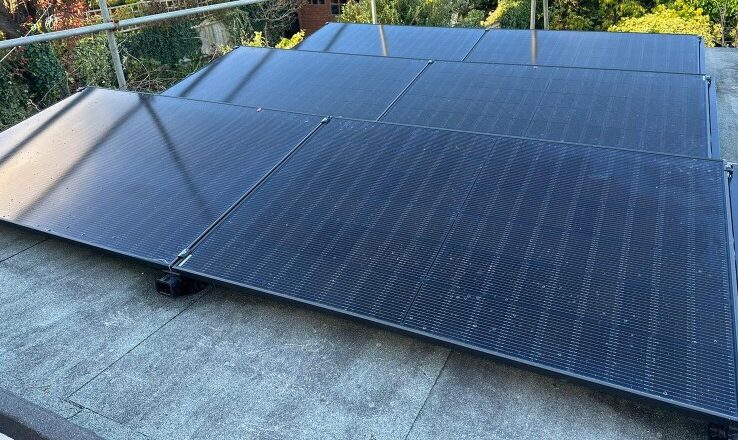
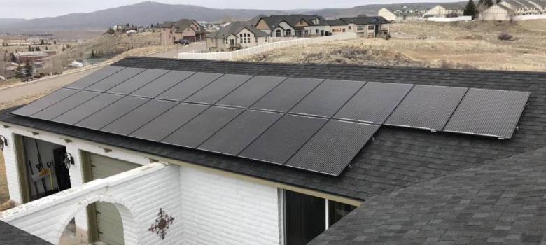
The most immediate and visual clue to identifying a monocrystalline solar panel is its distinctive color. While often simply described as "black," the specific shade and uniformity are direct results of the high-purity silicon used and the manufacturing process. Monocrystalline panels start as a single, cylindrical crystal of silicon, which is grown in a high-temperature furnace over a period of several days. This crystal is then sliced into thin wafers, typically around 180 micrometers (0.18 mm) thick. The high purity and single-crystal structure allow light to interact with the silicon in a very consistent way, absorbing a broader spectrum of light rather than scattering it. This fundamental property is why a monocrystalline panel appears as a deep, uniform black, even from an angle. In contrast, polycrystalline panels, made from multiple silicon fragments melted together, have a bluish, speckled appearance due to light scattering off the crystal grain boundaries. This visual difference isn't just about aesthetics; it correlates directly with higher efficiency rates. Monocrystalline panels commonly achieve cell efficiencies between 20% and 23%, while polycrystalline panels typically range from 15% to 18%.
l Look for a deep, uniform black hue.A true monocrystalline panel will have a very consistent color across its entire surface, with minimal variation. The surface should look like a single, seamless sheet of black material.
l Observe the anti-reflective coating.Modern monocrystalline panels are coated with a layer that minimizes glare and maximizes light absorption. This coating often gives the panel a non-glossy, matte finish. If you tilt the panel, the color should remain a consistent black without shifting to a noticeable blue or silver sheen. This coating can increase light absorption by over 3%, directly boosting energy output.
l Check for a solid color under the glass.Sometimes, the backing sheet (the rear surface of the panel) is white. Focus your inspection on the solar cells themselves, which are visible beneath the front glass. The cells should be a single, solid color. If you see a speckled or flakey pattern with shades of blue and silver, you are almost certainly looking at a polycrystalline panel. The random alignment of the multiple silicon crystals in a polycrystalline cell creates that distinctive mosaic effect, which can reduce efficiency by 2-4 percentage points compared to a monocrystalline cell of the same size.
This method is more energy-intensive and results in some silicon waste, which historically contributed to a 5-10% higher manufacturing cost per wafer compared to the casting method used for polycrystalline silicon.
Look for a Consistent Texture
Beyond color, the surface texture of a solar panel provides a critical, tactile clue to its manufacturing technology. The texture is a direct result of how the silicon wafers are produced. Monocrystalline silicon wafers are cut from a single, cylindrical crystal ingot, typically using a diamond-wire saw process that results in an exceptionally uniform surface. This process creates wafers with a predictable and consistent texture, which is then often enhanced with chemical etching to form a microscopic pyramidal structure. This texture is not just for show; it is engineered to reduce light reflection from over 30%on a flat surface to less than 2%, significantly boosting the panel's ability to trap photons.
Each wafer in a monocrystalline panel is a perfect replica of the next, leading to a homogeneous appearance. This uniformity is crucial for performance. Because every cell has an identical structure, electrons can flow with less resistance. This translates directly into higher efficiency; premium monocrystalline panels can reach efficiencies of 22% to 24%, while the inconsistent crystal boundaries in polycrystalline panels can hinder electron flow, capping typical efficiencies at around 17% to 19%.
The texture of a monocrystalline cell is not perfectly smooth. It features a microscopic pyramid texture created through a process called anisotropic etching. These pyramids, typically 5 to 10 micrometers in height, are designed to bounce incoming light around inside the silicon, increasing the probability of absorption and energy conversion by over 40%compared to a flat surface.
The diamond-wire slicing produces wafers with a consistent thickness of about 180 micrometers (0.18 mm)with a thickness variation of less than ±10 micrometers. This precision minimizes mechanical stress and micro-cracks that can develop in less uniformly textured wafers, contributing to the longer operational lifespan of monocrystalline panels, which often have performance warranties guaranteeing 90% output after 10 years and 80% to 85% after 25 years. The initial silicon ingot growth process, which takes over 48 hours at temperatures exceeding 1400°C, ensures the atomic structure is perfectly aligned.
Find the Nameplate and Model
While visual inspection provides good clues, the most definitive way to confirm your solar panel's technology is by checking its nameplate. This metal or plastic label, permanently attached to the panel's frame, is the authoritative source of its technical identity. International standards, such as IEC 61215, require manufacturers to include specific data. The nameplate contains encoded information that tells you exactly what you own, moving beyond guesswork to certified specifications. Locating and interpreting this label is a simple, 30-second process that yields 100% accurate results regarding the panel's construction, power rating, and operational limits.
Parameter on Nameplate | Typical Value for a 400W Monocrystalline Panel | What It Tells You About the Technology |
Model Number | e.g., "ABC-400M-144" | Often contains codes like "M" for Mono or "N-Type" for advanced monocrystalline. |
Maximum Power (Pmax) | 400 Watts | High power per panel (over 380W) is almost exclusive to monocrystalline. |
Cell Efficiency | 20.5% to 22.8% | Efficiencies above 20% strongly indicate monocrystalline technology. |
Open-Circuit Voltage (Voc) | ~40-50 Volts | Higher voltage per cell is a characteristic of pure silicon crystals. |
The label is designed to withstand outdoor exposure for over 25 years, but it may accumulate dust. Wipe it clean with a dry cloth to ensure all small print is readable. The model number is your primary key. Manufacturers deliberately use specific prefixes or suffixes. A code like "M-400" or "MONO-144" explicitly states the technology. A "P" or "POLY" indicates polycrystalline. Many modern panels use an alphanumeric code; searching for this full model number online for less than 2 minutes will almost always bring up the original data sheet from the manufacturer's website, providing absolute certainty.
While there are exceptions, a panel rated for 380 Watts or higher is almost certainly monocrystalline because achieving that high a power output from a standard 1.6 m² to 2.0 m²panel area requires the superior efficiency of a single-crystal silicon structure. Polycrystalline panels of the same physical size typically max out around 330W to 370W.
If the nameplate shows an efficiency of 20.5% or greater, you are unequivocally looking at a monocrystalline panel. The nameplate also provides the panel's electrical characteristics, such as the open-circuit voltage (Voc) and the temperature coefficient of power. Monocrystalline panels generally have a slightly higher Voc, around 0.5 to 1.0 volts more per string of cells, and a better temperature coefficient, typically around -0.30% to -0.35% per °C, meaning they lose less power output on a hot 45°C day compared to polycrystalline panels, which can have coefficients of -0.40% per °C or higher.
Notice the Shape of the Cells
Monocrystalline panels begin as a single, cylindrical crystal ingot grown using the energy-intensive Czochralski process, which involves slowly pulling a seed crystal from molten silicon at temperatures exceeding 1410°Cover a period of more than 72 hours. This results in a cylindrical ingot with a typical diameter of 200 mm or 210 mm. To maximize the usable area from this round ingot, the wafers are cut into a "pseudo-square" shape, which inevitably features subtly rounded corners. This process results in a silicon waste of approximately 15-20%from the original ingot. In contrast, polycrystalline silicon is cast in large rectangular molds, allowing for the creation of perfect squares with 90-degree angles and minimizing material waste to just 2-5%.
Cell Shape Characteristic | Monocrystalline Panel | Polycrystalline Panel |
Cell Corner Geometry | Rounded corners (pseudo-square) | Sharp, 90-degree square corners |
Visible Backsheet Pattern | Distinct diamond or rhombus-shaped gaps between cells | Thin, straight-line gaps forming a simple grid |
Material Utilization Efficiency | ~80-85% | ~95-98% |
For a standard 60-cell panel, this pattern appears 60 times. The cumulative area of these gaps represents a 3% to 5%loss of active surface area compared to a perfectly square layout. However, this is offset by the superior quality of the single-crystal silicon, which typically delivers a 1.5 to 3 percentage point higher conversion efficiency (e.g., 21.5%vs. 18.5%). This results in a net power gain for the monocrystalline panel, often yielding 20 to 40 more watts per panel of the same physical dimensions (approximately 1.7 meters by 1.0 meters).
A 120-half-cell module will display double the number of these diamond-shaped gaps, but the fundamental rounded-corner geometry remains the same. This design reduces resistive losses and can boost overall power output by 2% to 3%, while also improving performance in partial shade conditions. The presence of these rounded corners and the resulting diamond pattern on the backsheet is a over 95% accurate visual indicator of monocrystalline technology.
Compare with a Polycrystalline Panel
Monocrystalline panels use silicon with a perfectly aligned crystal lattice, achieving lab efficiencies that can exceed 24%, while polycrystalline panels, composed of multiple smaller crystals, have inherent boundaries that impede electron flow, capping practical efficiencies at around 17-18%. For a homeowner, this comparison translates into understanding tangible differences in power output per square meter, with monocrystalline panels typically generating 20-40 more watts per panel of the same ~1.6 m² to 2.0 m²size, a 5% to 10%power advantage that directly impacts the payback period of the system.
The monocrystalline panel will appear as a deep, uniform black, almost like a sheet of black glass. This is due to the single-crystal structure's ability to absorb a wider spectrum of light with minimal reflection. In contrast, the polycrystalline panel will have a speckled, bluish hue, often described as a mosaic or a shattered glass appearance.
Furthermore, if you can touch the panels after they have been operating in the sun for at least 30 minutes, you might notice a temperature difference. Polycrystalline panels generally operate at a 5°C to 10°C higher temperature than monocrystalline panels of the same size and under the same sunlight intensity.This lower operating temperature contributes to a slower rate of degradation; monocrystalline panels often have a lower annual degradation rate, typically 0.30% to 0.55% per year, compared to 0.50% to 0.80%for some polycrystalline panels.
Over a 25-yearwarranty period, this difference of just a few tenths of a percent can compound, meaning a monocrystalline panel might retain 3-5% more of its original output after two and a half decades. The initial price difference between the two technologies has narrowed to within 5-15%, making the long-term energy harvest advantage of monocrystalline a primary consideration.
Review the Manufacturer's Specifications
The data sheet, a comprehensive 2 to 4 page technical document, provides unambiguous specifications verified under standardized laboratory conditions (STC). These specs are not marketing fluff; they are grounded in IEC 61215 certification testing, which involves rigorous stress tests over several months, including 200 thermal cycles from -40°C to 85°C and exposure to 1000 W/m²of UV light.
Key Datasheet Parameter | Monocrystalline Indicator | Polycrystalline Indicator |
Cell Efficiency (%) | 20.5% and higher | Typically 17% - 19.5% |
Temperature Coefficient of Pmax (%/°C) | -0.30 to -0.35 | -0.38 to -0.45 |
Power Output (W) for a ~1.8m² Panel | 380W and above | 350W and below |
You can usually find it in less than 3 minutes by searching online for the panel's model number, which is found on the nameplate. The model number is a unique identifier; a code containing "M" (e.g., "ABC-400M") almost certainly denotes Monocrystalline, while a "P" indicates Polycrystalline. Once you have the data sheet, focus on three critical parameters. The cell efficiency is the most direct indicator. If the stated efficiency is 20.5% or higher, you are looking at a monocrystalline panel. Efficiencies in the 17% to 19.5%range are typical for polycrystalline technology. The second key parameter is the temperature coefficient of power.
Monocrystalline panels generally perform better in the heat, with coefficients around -0.34%/°C, meaning a panel rated at 400W will only lose about 13.6 watts of output when the cell temperature rises from the standard test condition of 25°C to a realistic operating temperature of 45°C. A polycrystalline panel, with a coefficient of around -0.42%/°C, would lose nearly 17 watts under the same conditions, a 25% greater relative power loss.