Can Damaged Portable Solar Panels be Repaired | Feasibility, Safety, Tools
Junction box or diode failures can be Troubleshot with a multimeter and repaired with a soldering iron.
However, if the silicon wafer is damaged, the conversion efficiency will plummet by more than 30%, posing a risk of hot-spot fires.
Due to the irreversible nature of physical damage, individual repair is generally not recommended when core cells are compromised.
Feasibility
Currently, the average price for mainstream 100W panels in the North American market is approximately $150 to $300, while the module cost for replacing a bypass diode or repairing a junction box is only $5 to $12.
If physical damage causes the open-circuit voltage (Voc) to drop by more than 15%, or if the cracked area of a single cell exceeds 10%, the power recovery rate after repair is typically lower than 75% of the original nominal value.
The repair success rate for damaged external wiring is nearly 100%, but for internal laminate damage, the success rate is less than 10%.
External Wiring Troubleshooting
Most outdoor folding panels use specialized photovoltaic cables certified by UL 4703 or TUV, with common specifications being 12 AWG or 14 AWG.
This multi-strand tinned copper wire design is intended to maintain flexibility while reducing resistance losses during high-current transmission.
Standard 12 AWG cable has a resistance of approximately 5.2 milliohms per kilometer at an ambient temperature of 20 degrees Celsius.
If the internal copper wires break by more than 30% due to frequent folding, local resistance will rise sharply, leading to significant heat generation when outputting currents of 8 to 10 Amperes.
According to physical thermal effects, when contact resistance increases to 100 milliohms, passing a 10 Ampere current generates 10 Watts of waste heat.
This is sufficient to raise the cable jacket temperature above 80 degrees Celsius, accelerating the aging of the insulation layer.
Due to the variable outdoor environment, cable jacket materials usually use XLPE (Cross-linked Polyethylene) or high-performance polyolefins.
These materials can withstand extreme temperature differences from -40°C to +90°C and possess UV (ultraviolet) resistance.
However, long-term UV exposure or chemical corrosion can cause the jacket to become brittle.
If fine, web-like cracks are found on the cable surface, it indicates that the insulation performance has declined, potentially leading to slight leakage currents in humid environments.
Use the 20 MΩ range of a multimeter to measure the insulation resistance between the positive/negative cables and the frame; a normal reading should be infinity.
If the reading is below 2 MΩ, it indicates that moisture has penetrated the sheath, and the damaged section must be cut out and resealed.
· MC4 Connector Loss Data: Standard MC4 terminals are rated for 30 Amperes, and contact resistance must be kept below 0.5 milliohms. If the internal shrapnel loses elasticity or oxidizes, contact resistance can soar to 5 milliohms or higher.
· Voltage Drop Test: In strong midday sunlight, measure the voltage at the junction box output and the MC4 interface at the end of the cable. If a 3-meter cable produces a voltage drop exceeding 0.3 Volts, it indicates serious metal fatigue or poor crimping within the cable.
· Plugging Life Limits: Ordinary MC4 connectors are designed for approximately 100 to 500 complete mating cycles. Frequently unplugging connectors under load generates an arc with instantaneous temperatures reaching thousands of degrees, causing burn pits on the metal contact surfaces.
· Sealing Grade Differences: Connectors with an IP67 rating can be immersed in 1 meter of water for 30 minutes without ingress. However, if the sealing ring (O-Ring) cracks due to dryness, moisture can enter the core through the capillary effect of the cable, causing the entire wire to blacken and oxidize.
Module Name | Common Specs/Parameters | Loss Manifestation | Recommended Repair Value |
PV Cable | 4 mm² (12 AWG) | Overheating, hardening jacket | Replace if resistance > 0.1 Ω |
MC4 Interface | 30A / 1000V DC | Blackened or melted terminals | Replace if contact resistance > 1 mΩ |
XT60 Plug | 60A Rated | Loose shrapnel, poor contact | Replace if insertion force is noticeably low |
Junction Box Seal | IP65/IP67 | Internal water accumulation, salt spray precipitation | Reseal if insulation resistance < 2 MΩ |
For 100W panels, 10 Ampere to 15 Ampere Schottky diodes are usually equipped.
The forward voltage drop of a Schottky diode is typically between 0.2 Volts and 0.4 Volts.
If the panel's output power drops by about 50% even without any shading, it is likely that one of the diodes has short-circuited.
A shorted diode bypasses an entire string of cells, causing the open-circuit voltage (Voc) to drop proportionally.
By testing with the diode setting of a multimeter, the forward voltage drop reading should be between 0.2 and 0.5, and the reverse should show no continuity.
If the junction box cover develops gaps due to external impact, moisture ingress will cause severe electrochemical corrosion.
In salt spray environments, a conductive path forms between the positive and negative busbars, generating a leakage current of 100 mA to 500 mA.
This hidden discharge not only wastes power but also generates heat that deforms the junction box.
When clearing such faults, 99.9% isopropyl alcohol should be used to thoroughly wash away the oxide layer, followed by filling with neutral electronic silicone adhesive. Once cured, this adhesive provides a dielectric strength of 18 kV/mm.
The silver-plated copper layer on Anderson plugs is typically 3 to 5 microns thick. If used frequently in sandy or seaside environments, fine sand particles will wear down the plating, exposing the underlying copper.
Once the protection of the silver layer is lost, the oxidation rate of the contact surface will increase by more than 10 times.
Under a full load of 15 amperes, a damaged plug's temperature will quickly climb above 65 degrees Celsius.
The criterion for determining if such an interface needs replacement is observing visible wear marks or black spots from electrical sparking on the metal surface.
If the plug feels loose, it usually indicates that the internal spring steel has annealed and lost its tension, failing to provide enough contact pressure to maintain low resistance.
The minimum bending radius for standard PV cables is usually 4 times the cable diameter.
For a 6 mm diameter cable, the bending radius should not be less than 24 mm.
During the storage of portable panels, if they are subjected to "dead folds" (180 degrees) long-term, the fine internal copper wires will undergo work hardening and fracture.
For every 10% of copper wire broken, the current density at that point increases by approximately 11%.
Observe the current output of the panel under constant light using a clamp meter. If the fluctuation amplitude exceeds 0.5 amperes and the reading jumps when shaking the cable, it indicates that the connection point is in a semi-broken state.
At this point, the cable should be cut 5 to 10 cm from the connector and re-crimped.
Recommended detection process for external wiring:
1. Disconnect from the energy storage power supply or controller to ensure an open-circuit state.
2. Measure the open-circuit voltage (Voc) and compare it with the factory parameter table. If the deviation is within 2 Volts, focus on troubleshooting wiring resistance.
3. Inspect the interior of the MC4 terminal for pale green (copper rust) or black (carbonized) substances.
4. Use an infrared thermal imager or manual sensation to confirm if the cable or junction box has local hot spots.
5. In a loaded state (such as charging a power bank), measure the potential difference before and after the connector.
Manual crimping force usually needs to reach over 1000 Newtons to ensure a cold-welded connection between the metal terminal and the cable.
If ordinary needle-nose pliers are used for crimping, tiny gaps will exist in the contact surface, allowing air to enter and trigger oxidation.
Correct repair involves stripping about 10 mm of insulation, ensuring the copper core is clean, placing it in the terminal, and crimping it firmly in one go.
After crimping, slip on a dual-wall heat shrink tube with internal adhesive and heat it to 120 degrees Celsius to melt the internal glue, providing long-term waterproof sealing.
This treatment can restore damaged external wiring to over 98% of its original transmission efficiency.
Repaired panels require a load stress test. Let the panel run at maximum output power for 30 minutes, checking the temperature of the junction box and connectors every 10 minutes.
At an ambient temperature of 25 degrees Celsius, the maximum temperature of these parts should not exceed 55 degrees Celsius.
Surface Coating Treatment
High-quality ETFE coatings have a light transmittance of approximately 95% and a refractive index of about 1.40, which effectively reduces reflection losses at the interface.
In contrast, cheaper PET coatings degrade under long-term UV exposure, typically showing significant yellowing after 500 to 1,000 hours of outdoor exposure. This leads to a 10% to 15% attenuation in short-circuit current (Isc).
Scratches deeper than 50 microns alter the angle of light incidence, creating a scattering effect that prevents photons from accurately hitting the underlying silicon wafer.
For slight wear on PET surfaces, using a fine polishing paste with a grit of 3,000 to 5,000 mesh for manual grinding can typically restore about 3% of power output.
However, for ETFE panels with a textured honeycomb structure, polishing may destroy the original light-trapping design, leading to a decrease in the absorption rate of low-angle light.
If a scratch has penetrated the protective layer and reached the silver paste grid lines on the cell, moisture in the air will enter through the crack, triggering a local oxidation reaction within 48 hours.
Coating Material Properties | ETFE (High Grade) | PET (Standard Grade) | Repair/Maintenance Suggestion |
Standard Transmittance | 94% - 96% | 80% - 85% | Demote use after PET yellows |
Surface Hardness (Shore D) | 65 - 72 | 75 - 80 | ETFE is tougher, higher impact resistance |
UV Resistance Life | 20+ Years | 3 - 5 Years | Cover PET with protective film if cracked |
Melting Temperature | 260°C | 250°C | Avoid heat guns exceeding 100°C |
Self-cleaning Angle (Water Contact) | Over 95° | 70° - 75° | Reduced angle means the coating has aged |
When the surface coating separates from the underlying EVA adhesive film, an air layer with a thickness of approximately 0.1 mm to 0.5 mm forms between them.
Since the refractive index of air is only 1.00, while the coating material is about 1.40, this refractive index mismatch results in a Fresnel reflection loss of approximately 4% at the interface.
If the delamination area exceeds 15% of a single cell's area, the power generation in that region will drop significantly.
The method to repair such faults is to use a syringe to inject low-viscosity optical-grade epoxy resin. By expelling air and re-establishing a physical connection, approximately 80% of local power loss can be recovered.
In high-salt spray environments such as the seaside, a high-resistivity film forms on the coating surface, blocking specific spectral bands.
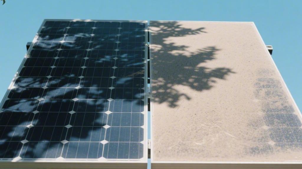
Experimental data shows that every 1 gram of dust accumulation per square meter results in a 4% to 7% drop in output power.
If solvents containing alcohol or acetone are mistakenly used to clean PET panels, they can cause the polymer material to swell or whiten, permanently reducing light transmittance by more than 20%.
The correct approach is to use demineralized water combined with a pH-neutral detergent.
For ETFE panels, due to their extremely low surface energy, a simple water rinse is usually sufficient to restore over 98% of the original light transmission performance.
Damage Condition | Physical Manifestation | Estimated Performance Loss | Repair Difficulty |
Slight Fogging | Loss of surface gloss | 5% - 8% | Low (Polishing) |
Deep Laceration | Exposed white EVA layer | 12% - 20% | Medium (Sealant patch) |
Large Area Delamination | Surface bubbles | 15% - 30% | High (Resin injection) |
Chemical Burn | Surface whitening/peeling | 40%+ | Extreme (Usually scrap) |
The bottom surface of portable panels usually employs TPT or TPE composite materials with a thickness of about 0.3 mm.
The main function of the backsheet is to provide DC insulation protection of over 1000 V.
If the backsheet is scratched by sharp stones, resulting in damaged insulation, the panel will produce micro-ampere level leakage currents when touching damp grass, triggering the controller's leakage protection.
Covering the area with specialized solar backsheet repair tape (usually containing Tedlar) can re-establish an insulation barrier complying with UL 1703 standards.
When repairing, ensure the tape extends at least 20 mm beyond the scratch edges and use a squeegee to remove air bubbles, ensuring the seal strength reaches over 40 pounds per inch.
When the ambient temperature rises by 1 degree Celsius, the efficiency of monocrystalline silicon cells typically drops by about 0.4%.
If the coating becomes rough due to aging, its thermal emissivity will drop from about 0.9 to 0.7, leading to heat accumulation inside the panel.
On a summer noon, an aged panel's internal temperature may be 5 to 8 degrees Celsius higher than a new panel.
By applying a layer of nano-scale hydrophobic heat-dissipation coating—costing about $15 in materials—the operating temperature can be reduced by about 3 degrees Celsius, indirectly improving power generation efficiency by 1.2%.
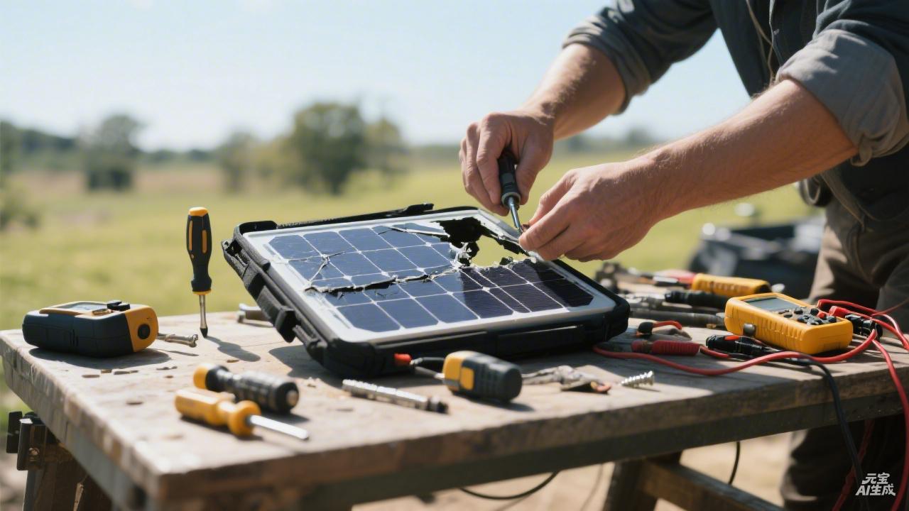
Internal Cell Damage
Portable solar cell thicknesses are usually between 160 and 200 microns.
This extremely thin monocrystalline silicon structure bears stress exceeding its mechanical strength limits during frequent outdoor moving, squeezing, or folding.
When a micro-crack exceeding 5 mm in length appears inside the silicon wafer, the current transmission path is physically interrupted.
According to laboratory electroluminescence test data, a micro-crack only 10 microns wide is sufficient to cause local resistance to jump from a normal 1 milliohm to over 50 ohms.
Since series circuits follow the principle of current consistency, a significant decay in the current of a single cell will forcibly limit the output of the entire cell array, causing the originally nominal 5.5 Ampere working current to drop below 2 Amperes.
Even if invisible to the naked eye, as long as the cumulative crack area accounts for more than 15% of a single cell, the panel's peak power output will suffer a permanent loss of over 25%.
The Young's modulus of silicon wafers is approximately 130 to 185 GPa. In portable application scenarios, if the local bending radius is less than 20 cm, the generated tensile stress will induce lattice dislocations. These dislocations diffuse in the high-temperature environment produced by light, causing the leakage current (Idark) to rise from nano-ampere levels to milli-ampere levels, significantly reducing the cell's open-circuit voltage.
When a cell's internal resistance becomes too high due to micro-cracks or partial shading, it converts from a power source to a load, consuming electricity generated by other normal cells.
This energy conversion generates heat concentrated in an area of a few square millimeters.
Measurement data shows that the temperature of the damaged area can soar from 45°C to 150°C or higher within 5 minutes.
This extreme heat exceeds the 80°C thermal stability threshold of EVA encapsulation film, triggering the thermal decomposition of the film and the release of acetic acid gas.
The acetic acid further corrodes the silver grid lines on the cell surface, thinning them from a normal 15 microns or even breaking them, eventually forming black oxidation spots.
In a 100W portable panel, there are usually 32 to 36 cells in series. If one cell's voltage drops by 0.5V due to a hot spot, because the bypass diode's turn-on voltage is typically between 0.3 and 0.6V, that diode will be frequently triggered. Long-term exposure to this high-frequency switching state causes the diode junction temperature to exceed 150°C, eventually leading to diode failure and leaving the entire panel without overheat protection.
For panels with multi-busbar (MBB) designs, although 9 or 12 busbars can share the current and reduce power loss from a single broken grid line, it also increases the precision requirements for manual repair.
Each busbar is only about 0.1 mm wide. When using an ordinary soldering iron for welding, the instantaneous temperature usually reaches over 300°C.
Due to the massive difference in thermal expansion coefficients between the silicon wafer and the metal solder ribbon, the thermal stress generated by welding often creates new micro-cracks around the solder joint.
This repair attempt often expands the damaged area, causing the original 10% power loss to increase to 30% post-repair.
In industrial standards, internal cell fractures are generally considered non-repairable.
The only physical remedy is using conductive silver paste to establish temporary current paths at damaged locations, but this introduces approximately 0.3 ohms of additional contact resistance.
Experimental data shows that cells repaired with conductive silver paste show a 50%+ drop in conductive layer peel strength after 10 thermal cycles from 0 to 60°C. In real outdoor temperature environments, the effective life of this repair method usually does not exceed 3 months.
Snail trails are another common internal chemical injury, appearing as brown streaks on the silver grid lines of the cell surface.
The physical basis for this phenomenon is the backsheet's water vapor transmission rate exceeding 5 grams per square meter per day.
When moisture enters and reacts with the silver grid lines, the produced silver ions migrate under the action of the electric field.
This electrochemical migration reduces the shunt resistance (Rsh) of the cell, making the panel's power generation capacity in low-light environments almost non-existent.
For a panel with a nominal voltage of 20V, if the shunt resistance drops from 1000 ohms to 100 ohms, the maximum power point voltage will deviate seriously, resulting in a 15% to 20% drop in matching efficiency with the MPPT controller.
Statistics show that portable panels used in environments with over 80% humidity are 4.5 times more likely to develop snail trails than those in dry areas. This damage is usually accompanied by an additional cell efficiency decay of 2% to 3% per year, much higher than the standard 0.5% rate.
If the cell suffers severe physical fragmentation—meaning fragment displacement exceeds 1 mm—the internal circuit structure has completely disintegrated.
In this case, the sharp edges of the broken silicon wafer produce point discharge phenomena, where local electric field strength may exceed the breakdown limit of air.
In dry air, this tiny arc continuously carbonizes the surrounding encapsulation material. Although the panel may still have voltage output, the current will exhibit extremely unstable fluctuations.
Through an oscilloscope, one can observe that the output current is filled with high-frequency noise, which can interfere with the charging circuit of the connected energy storage power supply or even cause the DC-DC converter to frequently restart due to abnormal input signals.
If the cost of optical glue, conductive materials, and labor time required for repair exceeds 40% of the price of a new panel, and the expected power recovery rate after repair is less than 80% of the original value, the behavior is economically irrational.
For most physical and chemical damage inside the cell, preventive protective measures, such as using high-strength support backsheets or limiting folding angles, are far more effective than post-damage remedies.
Safety
When operating 100W to 200W portable panels, even at low voltages of 18V to 22V, the instantaneous high temperature generated by a short circuit can exceed 200 degrees Celsius.
Before operation, the panel surface must be covered with a blackout cloth with nearly 0% light transmittance.
Repairs involving solder typically contain 37% lead and must be performed in an environment with a ventilation rate of at least 5 times per hour.
Using tools with a 1000V insulation rating is fundamental to prevent accidents when dealing with Direct Current (DC) arcs.
Preventing DC Arcs
Unlike the 120V or 230V Alternating Current (AC) common in North American or European homes, Direct Current (DC) does not have a zero-crossing point 100 to 120 times per second.
In AC circuits, the current periodically returns to zero, giving the air ionization layer a chance to cool and extinguish the arc.
When you forcibly unplug an MC4 or XT60 connector outputting 10A current under light, the air between the terminals ionizes instantly due to the high voltage, forming a plasma channel with a temperature between 3000 and 6,000 degrees Celsius.
This high temperature is sufficient to melt copper terminals (melting point 1085°C) and the outer PPO plastic insulation shell in less than a second.
Even a single 100W panel at around 18V is enough to maintain a stable arc several millimeters long.
DC Arc Physical Parameters | Typical Quantified Value | Physical Impact Description |
Arc Trigger Voltage | 12V to 20V DC | Visible sparks can be generated upon breaking the circuit at this range. |
Sustainable Arc Current | Greater than 0.5A | Below this, arcs extinguish easily; above this, arcs can stabilize. |
Arc Core Temperature | 3500K to 5500K | Far exceeds the melting points of steel and glass; contact points vaporize instantly. |
Air Breakdown Voltage | Approx. 3000 V/mm | Initial breakdown strength in dry air, though arc maintenance voltage is much lower. |
Plasma Impedance | Extremely Low | Once formed, resistance drops rapidly, leading to a current surge. |
When multiple portable panels are connected in series to increase voltage, the system's open-circuit voltage (Voc) typically reaches 60V to 75V.
According to the National Electrical Code (NEC), DC systems exceeding 80 V must be equipped with specialized Arc Fault Circuit Interrupters (AFCI), but civilian portable devices usually lack these complex electronic protection modules.
If micro-cracks exist in the busbar inside the panel, or if physical fatigue fracture of internal wires occurs during folding, a "drawing arc" phenomenon will occur as current passes through these breakpoints.
A fault point with only 0.1 ohm contact resistance will generate 10 watts of localized heat at a full load of 10 A.
This heat, concentrated in an area of less than 1 square millimeter, will cause the EVA film encapsulating the cells to thermally decompose and release flammable gases, thereby triggering a small-scale continuous fire inside the laminate.
Material Thermal Failure Threshold | Temperature Limit | Electrical Consequence After Damage |
EVA Encapsulation | 150°C | Bubbling and delamination; moisture ingress triggers large-scale shorts. |
PET Backsheet | 220°C | Structural carbonization; turns from insulator to semiconductor, leading to leakage. |
Tin-Lead Solder (60/40) | 183°C | Joints melt, causing physical open circuits and higher-energy arcing. |
PPO Plastic Shell | 170°C | Junction box deformation, resulting in seal failure and loss of IP rating. |
Monocrystalline Silicon | 1414°C | Physical melting; though the melting point is high, uneven heating causes cracking. |
Since silicon wafers react extremely quickly to light, indoor weak light alone is insufficient.
Covering the panel surface with black polyethylene (PE) blackout cloth over 0.1 mm thick or opaque canvas is the currently recognized standard.
Before disconnecting any connections, the open-circuit voltage at the output terminal must be tested with a digital multimeter rated CAT III 600V or CAT IV 300V.
Only when the voltage display is below 1V can the circuit be considered to lack sufficient energy to maintain an arc.
In coastal areas or humid forest environments, the silver-plated copper pins inside MC4 connectors are susceptible to salt spray corrosion.
When contact resistance increases from a normal 0.5 milliohm to 50 milliohms, the temperature rise at the contact point will accelerate significantly.
When the contact pressure is below 5 Newtons, vibrations from passing vehicles or wind jitter can cause thousands of micro-arc discharges per second inside the connector.
Handling Physical Debris
Portable panels are usually laminated from multiple layers of composite materials, including an outermost 0.025 mm to 0.1 mm thick ETFE or PET film, a middle EVA encapsulation layer, and monocrystalline silicon cells about 160 to 200 microns thick.
When a panel receives a point impact exceeding 50 Joules, the tempered glass layer or internal silicon wafers will suffer a shattering fracture.
As a brittle semiconductor material, silicon produces extremely sharp edges upon damage, with a Mohs hardness of about 7, enough to scratch most metal surfaces.
In dry environments, the dust particles generated by the fragmentation process typically range from 1 micron to 100 microns in diameter.
Material Composition | Physical/Chemical Characteristics | Exposure Risk Quantification |
Monocrystalline Silicon (Si) | High hardness, brittle, microscopic serrated edges | Generates PM2.5 level dust; can penetrate deep into the respiratory tract. |
Tempered Glass Shards | Particle size 2 mm to 10 mm | High stress; secondary shattering can occur when bending damaged panels. |
Busbar | Contains 36% to 40% Lead (Pb) | Lead oxide micro-particles from wear have neurotoxic properties. |
ETFE/PET Coating | Tough but prone to fine "hooks" | Can catch skin tissue, making wounds difficult to clean. |
Glass Fiber Substrate | Fine fibers, 5 to 15 microns diameter | Pierces the dermis, causing contact dermatitis or persistent itching. |
Since silicon dust is non-crystalline silica, long-term inhalation of such particles causes physical damage to lung tissue.
Using a vacuum cleaner with an H13 or H14 HEPA filter is recommended, as these devices can effectively trap 99.97% of particles exceeding 0.3 microns.
For tiny fragments embedded in fabric, high-tack polyethylene tape should be used for removal.
The ambient humidity during operation should be maintained above 50% to use the surface tension of water molecules to slow the floating speed of dust.
For handling large fragments, Level 5 cut-resistant gloves complying with EN388 must be worn; ordinary nitrile or latex gloves will be instantly sliced by silicon edges.
Eye protection must follow ANSI Z87.1 specifications, with full-seal side goggles.
When bending or carrying severely damaged folding panels, accumulated physical stress inside may cause fragments to suddenly eject outwards at initial speeds of up to 5 meters per second.
If a fragment enters the eye, rubbing is strictly prohibited because the microscopic hardness of the silicon will quickly scratch the cornea.
The correct procedure is to use sterile saline solution for low-pressure rinsing from the inner corner of the eye to the outer corner, using no less than 500 ml.
After processing physical debris, the repair area should be cleaned again using wet methods.
Use a damp microfiber cloth to wipe the surface, changing the cloth face every 0.5 square meters to prevent shards from scratching the workbench's protective layer.
PPE Specification | Technical Standard | Protection Detail |
Respiratory Protection | N95 or P100 Grade | Filters fine silicon dust and solder oxide particles. |
Cut-resistant Gloves | ANSI Level A5 or higher | Resists penetration by extremely sharp silicon wafers under 0.2 mm thick. |
Safety Goggles | Side-sealed, Impact D3 grade | Prevents fragment ejection or liquid splashes into the orbit. |
Protective Clothing | Polypropylene (Disposable) | Avoids microscopic glass fibers attaching to regular clothes and causing secondary allergies. |
Special attention must be paid to the spread of chemical contamination when handling lead-containing solder dross.
Portable panel busbars are typically dip-soldered using tin-lead solder. When a panel undergoes severe physical deformation or high-temperature burning, solder joints may turn into loose particles.
Such particles will slowly oxidize under the action of moisture if they enter the living environment.
When collecting such debris, a 6-mil thick polyethylene bag specially marked "Electronic Waste" or "Hazardous Substances" should be used for double-layer encapsulation.
In regions such as Europe and the US, such debris is generally not allowed to be disposed of as ordinary trash and must be sent to a recycling point with WEEE directive processing qualifications.
Operators should wash their hands and arms with a specialized lead-removal soap after finishing work; these soaps contain chelating agents that effectively remove heavy metal particles from skin texture.
Regarding common ETFE film damage in portable panels: if the cells under the film have shattered into particles smaller than 1 mm, the area has lost physical stability.
Even if the outer film is repaired with sealant, internal fragments will continuously wear down adjacent intact cells during thermal expansion and contraction cycles.
The inconsistency of thermal expansion coefficients will cause fragments to produce tiny displacements during daily temperature cycles (e.g., from 5°C at dawn to 65°C at noon).
Mechanical friction from these displacements further destroys the EVA layer, allowing moisture to enter through microscopic channels.
Experimental data shows that panels containing fragments have leakage currents over 400 times higher than normal panels after 48 hours of exposure to 85% humidity.
Therefore, for areas with overly dense physical fragments, the depth of physical cleaning should reach the substrate layer.
Thermal Management During Welding
Portable panels are usually composed of monocrystalline silicon wafers 160 to 180 microns thick tightly laminated with multiple polymer layers (e.g., ETFE, EVA, PET).
When welding busbars or cell ribbons, the soldering iron tip temperature is typically set between 320°C and 350°C.
If welding time exceeds 3 seconds, heat quickly conducts from the solder joint through the copper-based ribbon (thermal conductivity approx. 385 W/mK) to the surrounding EVA encapsulation.
When the EVA layer temperature exceeds 150°C, its internal molecular chains undergo thermal degradation, releasing corrosive acetic acid.
This chemical cannot escape the sealed laminate structure and will slowly corrode the cell's silver paste grid lines over the next 6 to 12 months, leading to irreversible power decay.
Welding Phase Parameter | Target Value/Metric | Consequence of Deviation |
Iron Tip Temperature | 320 to 350°C | Below 300°C causes cold joints; above 380°C burns cell PN junctions. |
Single Point Heat Duration | ≤ 2.5 Seconds | Timeout causes EVA vaporization, forming permanent bubbles > 1 mm. |
Solder Alloy Ratio | 62% Sn / 36% Pb / 2% Ag | Silver prevents the cell's silver paste from being "eaten" by solder. |
Heat-affected Zone Radius | < 3 mm | Limiting heat protects the electrical integrity of adjacent cells. |
Contact Pressure | 2 to 5 Newtons | Excessive pressure causes micro-fractures in 160-micron silicon. |
Instantaneous high temperatures from welding must be strictly monitored by physical isolation equipment. On the back of the damaged panel, a ceramic fiber board or specialized welding insulation mat at least 5 mm thick should be used as support to prevent heat from penetrating the backsheet and melting the outer fabric or plastic supports.
The expansion coefficient of copper is about 16.5 μm/m·K, while monocrystalline silicon is only 2.6 μm/m·K.
In the process of the solder joint temperature dropping sharply to room temperature, massive thermal stress is generated.
If flexible tin-coated copper ribbons are not used, this stress acts directly on the silicon lattice, producing micron-level cracks.
According to infrared thermal imager data, a cell with such micro-cracks will show significantly higher local resistance at rated current (e.g., 8A), and the resulting Joule heat will cause local temperatures to be over 15°C higher than surrounding areas.
As outdoor environmental temperatures fluctuate from 0°C at dawn to 70°C at noon, repeated thermal expansion and contraction cause micro-cracks to extend, eventually causing the busbar to peel off the cell surface.
Material Category | Linear Expansion Coefficient (10^-6/K) | Thermal Conductivity (W/mK) | Welding Process Impact |
Monocrystalline Silicon | 2.6 | 148 | Brittle; cannot withstand sharp local thermal gradients. |
Tin-coated Copper Ribbon | 16.5 | 385 | Fast cooling/contraction easily pulls cell surface. |
ETFE Layer | 135 | 0.24 | Huge expansion coefficient; heat causes offset in encapsulation. |
Tin-Lead Solder | 24.5 | 50 | Cooling speed determines grain structure; slow cooling reduces strength. |
EVA Encapsulant | 180 to 200 | 0.35 | Softens easily; loses structural support above 80°C. |
When choosing no-clean flux, one must confirm it is halogen-free. Halogen ions act as electrolytes in hot/humid environments, inducing galvanic reactions that cause solder joint resistance to surge from 0.01 ohm to over 1 ohm within a single summer. At 100W output, this 1-ohm resistance wastes 8 to 15 Watts of power, converting it into waste heat enough to melt plastic covers.
Before formal welding, a far-infrared preheating station can be used to slowly raise the damaged area's temperature to 60°C.
This approach narrows the temperature difference between the iron tip and the substrate, thereby reducing the contact time required for welding.
For surface-mount diodes (SMD) common in portable panels, a heat gun set to airflow level 3 and 320°C should be used for non-contact heating.
Since the diode package volume is only about 5 mm x 8 mm, excessive heating causes thermal breakdown of the internal semiconductor chip.
After welding is complete, the joint should naturally cool for at least 60 seconds; using compressed air or water for forced cooling is strictly prohibited.
Forced cooling leads to numerous micro-pores and cracks inside the solder, reducing its shear strength by over 40%.
Tools
Portable panel repair relies on a 0.1V precision multimeter to detect 12V to 48V open-circuit voltage deviations.
Circuit repair requires a 60W constant-temperature soldering iron operating at 320°C to ensure 0.3 mm thick busbars are firmly connected.
Surface repair requires specialized ETFE tape with a thickness of 0.15 mm and 91% light transmittance, used alongside 99% isopropyl alcohol for degreasing. All operations must comply with IEC 61215 performance standards.
Electrical Status Detection Tools
In electrical diagnosis of portable solar panels, a digital multimeter must have a DC voltage accuracy of 0.1% or higher and a CAT III 600V safety rating.
When measuring Voc for 12V or 24V nominal systems, a model with over 6000 counts is recommended to capture subtle 0.01V fluctuations.
In full sunlight approx. 800 to 1,000 W/m², if the measured voltage is more than 15% below nominal, it typically reflects cold solder joints or diode breakdown in the series loop.
When measuring short-circuit current (Isc), the multimeter leads must support sustained currents of over 10 A, and the internal resistance must be below 0.05 ohms.
High-power panels generate visible arcs during testing; operators should wear Class 0 insulation gloves.
By comparing current output at different light angles, one can quantify the loss of light transmittance due to UV aging of the encapsulation layer, which typically ranges from 1% to 3% annually.
Measurement Device | Recommended Precision/Range | Diagnostic Indicator | Normal Deviation Range |
High-Precision Multimeter | 0.1% DC / 10A DC | Voc and Isc measurements | Voltage deviation < 10% |
Infrared Thermal Imager | Res. 160 * 120 / Sens. 40 mk | Local hot spot detection | Temp difference < 15°C |
Solar Irradiance Meter | Range 0 - 1,500 W/m² | Real-time light intensity | Error < 5% |
Adjustable DC Load | 150 W / 60 V | IV characterization | Power deviation < 20% |
Infrared thermal imagers play an irreplaceable role in non-destructive testing.
Due to frequent folding, the silver busbars inside portable panels are prone to metal fatigue.
The IR spatial resolution should not be less than 19200 pixels, and thermal sensitivity must reach 0.04°C.
While the panel is under load (e.g., charging a 100Wh outdoor power supply), damaged cell regions convert kinetic energy into thermal energy due to increased resistance.
Normal cell temperature differences should stay within 5°C. If bright white spots appear in the thermal image with temperatures exceeding ambient by 20°C, it indicates micro-cracks or oxidized solder joints.
For ETFE surfaces, the imager's emissivity must be manually set to about 0.85 to avoid temperature measurement errors.
To obtain repair data with comparative value, a Solar Irradiance Meter is the basis of standardized testing.
Non-professionals often mistakenly believe that sunny weather is enough for testing, but cloud cover or Air Mass (AM1.5) changes can cause the output power of the same panel to fluctuate by 200 W/m² within ten minutes.
Using a silicon-sensor type irradiance meter ensures a wavelength response consistent with monocrystalline panels, covering a range of 400 to 1,100 nm.
During repair, measure environmental irradiance first. If the actual value is 500 W/m², a nominal 100W panel has a theoretical maximum output of only 50W.
If the multimeter shows only 30W, the panel has a 40% power deficit, which exceeds diode losses and requires checking internal connections.
Cable & Connector Module | Technical Specification | Electrical Impact | Inspection Standard |
MC4 Test Lead | 10 AWG Tinned Copper | Line loss resistance < 0.1 Ω | No burn marks on contact points |
Bypass Diode | 15A 45V Schottky | Forward drop < 0.55V | Reverse leakage < 1mA |
Alligator Clip Adapter | Thickened Pure Copper | Contact resistance 2 mΩ | Spring pressure > 5 Newtons |
By manually or automatically adjusting impedance, one can observe the current path from zero voltage (short circuit) to maximum voltage (open circuit).
A healthy portable panel has a distinct knee near the maximum power point (Pmax).
If the IV curve shows a step-like drop in the middle, it indicates that a group of cells in parallel branches has been isolated by a bypass diode, usually triggered by local shading or severe cell damage.
The length of cables used during testing should be kept under 1.5 meters, and the wire gauge should be no less than 12 AWG to avoid line resistance interference.
For panels equipped with USB-C or DC 5521 ports, a PD 3.0 protocol decoy trigger is also needed to ensure internal buck circuits do not skip frequencies due to overheating under 20V 5A high load.
When measuring internal junction box voltage, ultra-fine probe tips with a diameter under 0.5 mm are needed to pierce the surface moisture-proof coating.
If a 0.1-ohm contact resistance exists at the test point, it will produce a 0.5V drop at 5A current, which is enough to mislead the assessment of cell health.
For panels used frequently at the seaside or in humid environments, the silver plating inside MC4 connectors must be checked for oxidation.
Use a 30x industrial magnifier with an LED light source; if black sulfides are found, treat them with precision electronic cleaner before testing, as erroneous impedance data will lead to incorrect repair plans.
Circuit Solder Repair Equipment
For electrical repair of portable panels, constant-temperature soldering iron power must be maintained between 60W and 80W to handle the extremely fast heat dissipation of solar cells.
Ordinary low-power irons will have their heat quickly dissipated by the silicon wafer and backsheet upon touching a large busbar, preventing the solder from melting completely and forming high-resistance cold joints.
It is recommended to set the temperature between 320°C and 350°C and use a 2.4 mm or 3.2 mm Chisel tip.
This flat contact tip provides a larger surface area to complete heat transfer within 2 to 3 seconds, avoiding thermal stress fracturing of the monocrystalline silicon wafer from prolonged heating.
Welding Equipment/Material | Technical Requirement | Electrical/Physical Attribute |
Constant-Temp Soldering Iron | Power 80 W / Temp Error ±2°C | Ceramic heating core / ESD Protection |
Solder Wire | Sn63/Pb37 or SAC305 | Dia. 0.8mm / 2% Rosin core |
Flux | Weak active No-Clean (RMA) | Solid content 3-5% / Halogen-free |
Pre-tinned Busbar | Width 2.0mm / Thickness 0.15mm | Oxygen-free copper / 25μm coating |
In handling damaged circuit connections, the choice of solder determines the vibration resistance of the joint. Portable panels are used for outdoor mobile scenarios and endure frequent folding and vibration. Choosing a 63/37 eutectic solder wire ensures the joint transitions directly from liquid to solid upon cooling, reducing lattice displacement during a semi-molten state.
Since the silver paste layer on cell surfaces produces an oxide film after exposure to air, the application of a Flux Pen is essential.
Before welding broken ribbons, apply a layer of no-clean flux with about 3% solid content evenly on the pad area.
This liquid strips the oxide layer from the metal surface at medium temperatures, reducing the tension of liquid solder so it spreads smoothly across the 2.0 mm wide busbar.
Avoid using strongly acidic industrial soldering pastes, as residues will cause severe electrochemical corrosion in humid field environments, rendering the circuit useless within six months due to resistance surge.
· Interconnect Busbar Ribbon: Use 99.9% pure oxygen-free copper as base material, pre-tinned evenly with 20 to 40 microns of tin-lead alloy. Choose 1.5 mm or 2.0 mm width depending on specs; yield strength should be below 80 MPa to ensure it doesn't tear the cell electrode when the flexible panel bends.
· Schottky Bypass Diode: If protection modules in the junction box break down, replace them with 15A or 20A units. Reverse voltage rating should be 45V+, and forward drop below 0.55V.
· 12 AWG Tinned Copper Wire: External output cables face UV aging and mechanical wear. Choose UL 4703 compliant PV cables wrapped in XLPE insulation, maintaining flexibility from -40 to 90°C.
For insulation protection after welding, dual-wall adhesive heat shrink tubing provides a seal rated IP67 or higher. These tubes usually have a 3:1 or 4:1 shrink ratio with an inner wall lined with EVA hot-melt glue. At 125°C heat, the inner glue melts and fills cable gaps, forming a physical barrier against salt spray and moisture, keeping contact resistance below 0.5 milliohms long-term.
During junction box maintenance, Solder Suckers and Stainless Steel Tweezers are precision tools for positioning.
A manual pump-style solder sucker quickly removes excess solder from old cell connections, preventing excess tin balls from piercing encapsulation during folding and causing shorts.
For fine 2.0 mm busbars, use ESD-coated pointed tweezers to precisely control welding position, ensuring an overlap length of at least 5.0 mm.
Consumables/Parts | Specification | Environmental Resistance |
Heat Shrink (Adhesive) | Dia. 6mm / 3:1 Ratio | Waterproof to 1m / UV Resistant |
MC4 Connector | 30A / 1500V DC | Flame retardant UL 94-V0 |
Insulating Coating | Acrylic based / 10kV Breakdown | Salt spray resistant / High transparency |
Electronic Cleaner | 1,1-Dichloroethane mixture | Zero residue / Fast evaporation |
In some portable panel PCB repairs, especially involving USB control circuits, Low-Temperature Solder Paste is required.
Since these boards are usually inside plastic housings, 138°C melting point tin-bismuth alloy paste allows module reinforcement at lower temperatures, effectively protecting the plastic support structure from thermal collapse.
After repair, spraying a layer of Acrylic Insulating Varnish about 50 microns thick on all exposed electrical connections provides extra moisture protection, ensuring the panel doesn't suffer output fluctuations due to surface leakage after rain.