What is the Difference Between a Solar Cell and a Solar Panel
Solar cells are micro-sunlight conversion units that generate a voltage of about 0.5 V, while solar panels are macro-modules that encapsulate 60 or 72 cells in series and parallel under tempered glass.
Their standard output power is usually above 400 W, making them practical power generation systems that combine weather protection and large-scale power production.
Structure and Composition
The current mainstream 182 mm specification silicon wafer has an area of 331.24 square centimeters.
Through phosphorus or boron doping, a PN junction is formed inside the wafer.
Under the standard solar intensity of 1,000 Watts per square meter, a single cell can generate an open-circuit voltage of approximately 0.62 Volts.
Although the laboratory efficiency of N-type TOPCon cells has reached 26.7%, the average efficiency on large-scale mass production lines is typically maintained between 24.8% and 25.2%.
Each silicon wafer produces about 30% kerf loss (offcut waste) during the cutting and processing stages.
Its brittleness is extremely high; an edge curvature exceeding 2 mm will cause stress fractures, which is why it must be protected.
The Core Thin Wafer
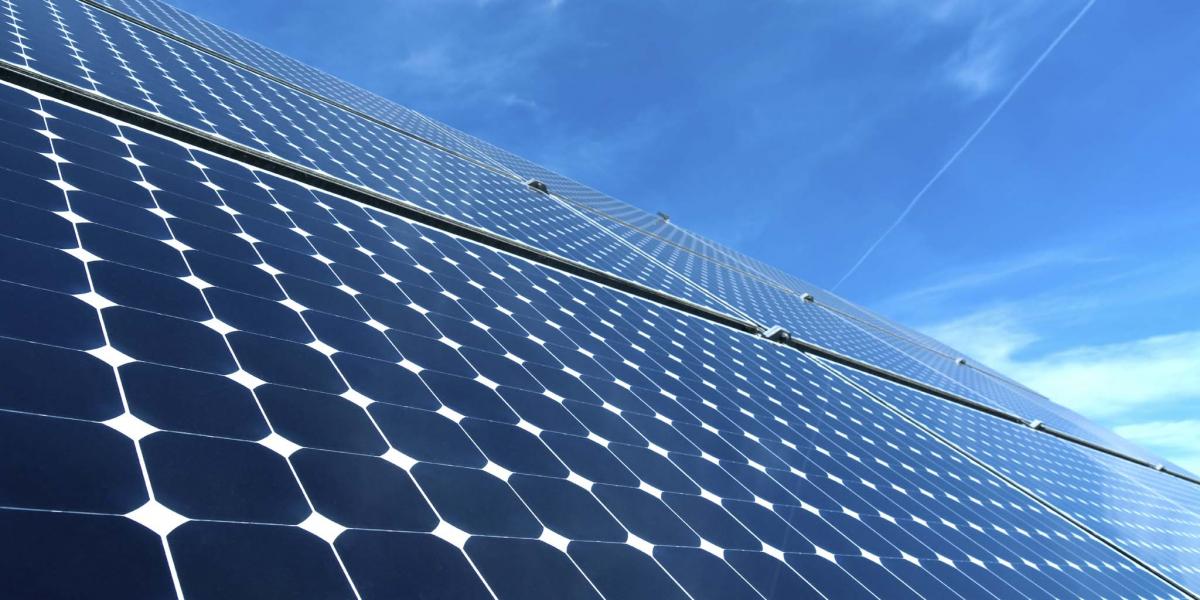
The solar cell is the "energy heart" of the photovoltaic module, and currently, monocrystalline silicon occupies more than 90% of the market share.
The rated current of a single 182mm cell is around 13 Amperes, but its voltage is extremely low, at only about 0.6 Volts.
If you want to charge a 5-volt mobile phone, you would need to connect at least 10 cells in series.
To improve light absorption, the cell surface is chemically etched to create pyramid-shaped textures with a height of about 3 to 5 microns.
This micro-nano structure can reduce reflectivity from 35% to below 10%.
The width of the silver paste grid lines on the cell surface has been reduced to within 30 microns to minimize sunlight shading.
The cost of silver paste per cell accounts for approximately 15% of the total cell cost.
Like a Sandwich
The outermost layer is 3.2 mm thick ultra-clear patterned tempered glass. This glass has an iron content of less than 150 ppm, ensuring a light transmittance of over 91.5%.
The top and bottom layers of the cell are covered with 0.45 mm thick EVA or POE film. These polymer materials undergo a cross-linking reaction after being heated for 15 minutes in a vacuum laminator at 145 degrees Celsius, tightly encapsulating the cells.
The bottom layer is a 0.3 mm thick composite backsheet made of fluorine film and PET materials, possessing an insulation dielectric strength of over 3000 Volts.
This five-layer superimposed structure increases the impact resistance of the entire panel by more than 100 times, enough to withstand a direct hit from a hailstone 25 mm in diameter traveling at 23 meters per second.
How the Wires Connect
Mainstream MBB (Multi Busbar) technology uses 16 circular tin-plated copper ribbons with a diameter of 0.25 mm, which reduces the shading area by 25% compared to the older 5-busbar technology.
The total length of 60 or 72 cells after series connection is usually between 1.7 meters and 2.2 meters. The thermal loss generated by internal resistance must be controlled within 2%.
When the ambient temperature rises, cell efficiency exhibits a negative temperature coefficient; for every 1 degree Celsius increase, the output power drops by about 0.35%.
To deal with the hot spot effect caused by shading, the junction box contains 3 built-in Schottky diodes with rated operating currents typically between 25 and 30 Amperes, ensuring that partial shadows do not burn out the entire panel, which is worth about 1,000 RMB.
The External Frame
The skeleton of the panel is a 6063-T5 grade aluminum alloy frame, with an oxide film thickness of over 15 microns to prevent salt spray corrosion.
The wall thickness of the frame is usually between 1.1 mm and 1.3 mm, with a height of 30 mm or 35 mm.
This structure not only provides support but also allows the module to withstand a static snow load of 5400 Pascals on the front and a wind pressure of 2400 Pascals on the back.
During installation, the 8 mm diameter mounting holes at the bottom of the frame ensure a heat dissipation gap of more than 10 mm between the module and the bracket.
For a 550W module weighing 28 kg, the aluminum frame accounts for about 15% to 18% of the weight, but it provides structural stability for over 25 years, ensuring that the deformation of the internal silicon wafers is less than 1% under a 30 kg load.
How Much Electricity Is Converted?
A single 550W panel is usually composed of 144 half-cut cells.
Half-cut technology reduces the cell current by half. According to Joule's Law ($P = I^2 R$), the internal resistance loss is reduced to 25% of the original.
The Fill Factor (FF) of the module is typically between 78% and 82%, which is an important parameter for measuring the quality of the solar panel.
Under Standard Test Conditions (STC) at 25 degrees Celsius, a 2.6 square meter module can produce 0.55 kWh of electricity per hour.
Considering an inverter efficiency of 98% and 3% line loss, a 10 kW residential distributed power station in an area with 1,200 annual effective utilization hours will have a total first-year power generation of approximately 11,600 kWh.
Calculated at 0.4 RMB per kWh, the annual income can reach 4,640 RMB, with a payback period usually locked between 5 to 7 years.
How Many Years Will It Last?
In damp-heat testing, it must work continuously for 1,000 hours in an environment of 85 degrees Celsius and 85% humidity, with power degradation remaining below 5%.
Linear warranties from reputable manufacturers usually cover 25 to 30 years.
The first-year power degradation is controlled within 1% to 2%, and the subsequent average annual degradation rate is between 0.45% and 0.55%.
By the 25th year, this panel can still maintain more than 84.8% of its original rated power.
Even in a desert environment at 50 degrees Celsius, the leakage current of its backsheet must be lower than 0.1 microamperes per square meter.
This weather resistance is something a single cell completely lacks and is the basis for large-scale PV investments to achieve an annualized return of over 15%.
Power Capacity
If you are holding a 182 mm monocrystalline silicon cell, its rated power is typically only 7.5 to 9 Watts.
In a laboratory Standard Test Condition (STC)—that is, under a light intensity of 1,000 Watts per square meter—the current generated by this wafer is approximately 13 to 14 Amperes, while its voltage is very low, stabilizing at around 0.6 Volts.
If you want this cell to drive a smartphone charger with a rated voltage of 5 Volts, you must find at least 8 such cells to connect in series.
The power generation capacity of a single cell is extremely limited by its physical size and the bandgap width of the semiconductor material.
Currently, the theoretical efficiency limit for monocrystalline silicon is around 29.43%, while mass-produced cell efficiencies have generally reached the range of 24.5% to 25.5%.
A single 182 mm cell has an area of about 331 square centimeters. In a standard environment of 25 degrees Celsius, its short-circuit current can reach 13.8 Amperes and its open-circuit voltage is about 0.72 Volts.
How Much Power Exactly?
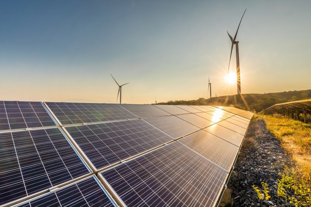
Currently, the power of mainstream large-format modules on the market has crossed 550 Watts and has even reached a new height of 670 Watts.
A 550W panel of approximately 2.5 square meters can generate 0.55 kWh of electricity per hour under peak sunlight.
In a region with abundant solar resources, such as one with 1,400 annual effective utilization hours, the total annual power generation of a single panel is approximately 770 kWh.
This increase in scale is achieved through the series-parallel structure of the cells, which raises the output voltage to a range of 40 to 50 Volts. This voltage range allows string inverters to operate efficiently.
For a typical 10 kW home rooftop project, it is usually necessary to install 18 to 20 of these high-power modules, with an average daily output of 40 kWh.
Based on current average market prices, the cost per watt for a module is about 1.1 to 1.3 RMB; a 550W panel costs around 650 RMB. Under ideal 5-hour sunlight conditions, its daily revenue is roughly equal to the market price of 2.5 kWh of electricity locally.
Where Is the Loss?
Although the conversion efficiency of the cell itself can reach 25%, after being encapsulated into a panel, the efficiency of the whole panel usually drops to between 21% and 23%.
There are many reasons for this approximately 1.5% to 2.5% efficiency drop.
First is the reflection and absorption of the cover glass. Even ultra-clear tempered glass with a transmittance of 91.5% will block some photons.
Second is the gap between the cells; these non-generating areas pull down the average power per unit area.
Added to this is the thermal resistance loss generated by the series connection of the ribbons. Every step in the process carves away some of the initial energy from that silicon wafer.
To reduce these losses, manufacturers use MBB technology and half-cut processes, halving the current to reduce internal resistance heat loss by 75%.
Modules using MBB technology reduce shading areas via 16 circular ribbons. Experimental data shows that this improvement can increase the module's Fill Factor by more than 1%, thereby increasing the output power of the whole panel by 5 to 10 Watts without increasing the silicon wafer area.
Is the Efficiency High?
Solar panels have a parameter called the temperature coefficient. Currently, mainstream P-type modules have a temperature coefficient of around -0.35%.
This means for every 1 degree Celsius the actual temperature of the panel rises above the standard 25 degrees Celsius, its power generation efficiency drops by 0.35%.
In the hot summer, rooftop panel temperatures can often soar to 65 degrees Celsius. At this time, the actual power of the panel will shrink by about 14% compared to the nominal power.
This is why at least 10 cm of ventilation space must be reserved at the bottom of the panel during system design.
In contrast, new N-type cell technology has better stability at high temperatures, with its temperature coefficient optimized to below -0.3%.
Over a 25-year lifecycle, this allows it to produce 3% to 5% more total electricity than traditional panels.
In a 50 kW small industrial and commercial project, choosing N-type modules with a better temperature coefficient can generate about 150 kWh more electricity in summer months than ordinary modules. Over 25 years, the extra revenue from this technical difference can cover the initial 5% premium investment.
Calculating the Finances
Taking a 20 kW distributed system as an example, the initial total investment budget is roughly between 60,000 and 80,000 RMB.
This system can generate about 26,000 kWh of electricity annually. If it is all for self-consumption, calculated at an electricity price of 0.6 RMB, it can save 15,600 RMB in electricity expenses per year.
Excluding annual O&M costs and equipment depreciation, the dynamic payback period of the system is locked between 4.5 and 6 years.
Considering that the solar panels have a 30-year lifespan, for the 20+ years after payback, they are essentially providing free clean energy.
This long-term economic benefit is built on the extremely low degradation rate of the panels. Usually, the first-year power degradation does not exceed 1%, and the subsequent annual linear degradation rate is controlled at about 0.4%.
Statistics show that high-quality monocrystalline modules can still maintain over 94.5% of their factory nominal power after 10 years of operation. Even in the 25th year, their actual power generation capacity remains at the 85% level, providing high certainty for long-term power asset evaluation.
When the Weather Changes
When cloud cover increases and irradiance drops from 1000 W/m² to 200 W/m², the output current of the module decreases linearly, but the voltage drop is relatively small.
This characteristic means that even on cloudy days, solar panels can still maintain about 10% to 15% of their power generation capacity.
To deal with low-light environments in the morning and evening, modern cell surfaces use light-trapping textured technology, increasing the reflection path of photons inside the silicon wafer.
When the early morning sunlight is only 100 W/m², advanced TOPCon modules can enter the inverter's startup voltage range 15 minutes earlier. This slight improvement in low-light response can accumulate to a 2% increase in total annual power generation revenue.
Protection and Longevity
The Hard Shell
The outermost layer of a solar panel is covered by a piece of ultra-clear tempered glass, usually 3.2 mm thick, which has undergone special physical strengthening treatment.
In impact tests, it can withstand a 25 mm diameter hailstone weighing approximately 7.5 grams hitting it frontally at a speed of 23 meters per second without cracking.
The light transmittance of this tempered glass is usually maintained between 91.5% and 93%, ensuring that the vast majority of photons penetrate and reach the cells below.
In addition to frontal protection, the surrounding aluminum alloy frame (about 1.5 mm thick) provides strong mechanical support, allowing the panel to withstand up to 5400 Pascals of frontal pressure. This is equivalent to piling 540 kg of snow on every square meter of area.
To prevent moisture infiltration, the cells are tightly wrapped by two layers of polymer film with a thickness of about 0.45 mm to 0.6 mm.
Currently, the mainstream encapsulation materials are EVA (Ethylene-Vinyl Acetate) or the higher-performance POE (Polyolefin Elastomer).
In the factory's vacuum laminator, these films melt at a high temperature of 145 degrees Celsius and undergo a cross-linking reaction, bonding the cells, glass, and the bottom backsheet together.
This sealing process allows the solar panel to work continuously for 1,000 hours in an environment with 85% humidity and 85 degrees Celsius, with power loss still less than 5%.
Protective Module | Key Specifications | Protection Description | Durability Metric |
Tempered Glass | 3.2mm / Ultra-clear Patterned | Resists hail and sand impacts | Transmittance > 91.5% |
Aluminum Frame | 6063-T5 / 35 mm High | Prevents deformation and stress | Snow Load 5400 Pa |
Encapsulation Film | 0.45 mm EVA/POE | Insulates and blocks moisture | Resistivity > 1E14 |
Composite Backsheet | 0.3 mm TPT/KPE | Resists UV and prevents leakage | Voltage Withstand > 1500V DC |
Junction Box | IP68 / Built-in Diodes | Heat dissipation; prevents hot spots | Rated Current 25A-30A |
Waterproof Performance
A qualified module must have a leakage current of less than 0.1 microamperes per square meter under a 1500 Volt DC high-voltage test.
To achieve this level of protection, the junction box on the back of the panel uses a potting compound filling process, reaching an IP68 protection rating. It can be immersed in 1.5 meters of water for 30 minutes without leaking electricity.
The junction box contains 3 Schottky diodes. When a cell generates local high temperatures due to shading by leaves, these diodes can quickly divert the current through a bypass circuit, preventing local temperatures from soaring above 150 degrees Celsius and causing the encapsulation material to carbonize.
During a 25-year operation cycle, solar panels also face an invisible threat called PID (Potential Induced Degradation).
When there is a high voltage difference of hundreds of volts between the panel frame and the cells, sodium ions will penetrate the encapsulation material into the silicon wafer, causing the output power to shrink by more than 50% in just a few years.
To combat this, modern panels use anti-PID POE film, whose water vapor transmission rate is only 0.2 grams per square meter per day, which is an order of magnitude lower than traditional EVA film.
Through this microscopic material improvement, the probability of unexpected downtime for modules over their lifecycle has been reduced to below 0.05%.
Enduring Thirty Years
After passing the initial degradation of the first year, the linear degradation rate of high-quality panels stabilizes between 0.4% and 0.55% per year.
After 25 years of installation and operation, your system can still maintain about 84.8% of its factory power generation capacity.
In contrast, the efficiency of an unprotected solar cell in an outdoor environment would drop to zero within weeks; the lifespan gap is more than 1,000 times.
To verify this ultra-long lifespan, every batch of panels must pass the TC200 (200 thermal cycles) test.
The test environment fluctuates violently between -40 degrees Celsius and +85 degrees Celsius, with each cycle taking about six hours to simulate the changing seasons over 25 years.
Under such harsh testing, the metal fatigue cracks in the panel's internal ribbons must be controlled at the micron level to ensure the increase in module internal resistance does not exceed 5%.
It is this almost harsh industrial encapsulation standard that allows PV power stations to become a stable financial asset, with an annual asset depreciation rate far lower than most traditional power generation equipment.
For offshore salt spray environments, professional panels increase the thickness of the anodic oxide film to over 15 microns. Experimental data shows that after passing the Level 6 salt spray test of the IEC 61,701 standard, the corrosion area of the module's metal grid lines should be less than 0.1%, ensuring that seaside power stations also have a 25-year investment return cycle.
Even in desert areas at 50 degrees Celsius, the module backsheet can resist strong UV radiation of more than 250 kWh per square meter annually without yellowing.
This UV resistance mainly comes from the fluorocarbon coating on the surface of the backsheet. Its chemical bonds are extremely strong and can effectively prevent high-energy photons from breaking the polymer chains.
Through these layers of protection, from microscopic materials to macroscopic structures, a 28 kg panel protects ultra-thin cells with a total weight of less than 500 grams, steadily turning sunlight into money under various harsh natural conditions.