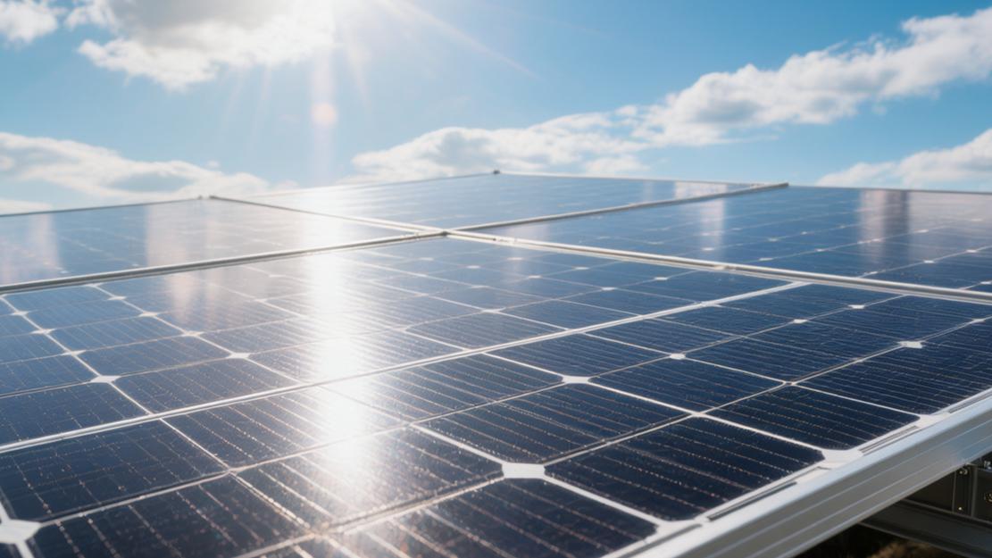
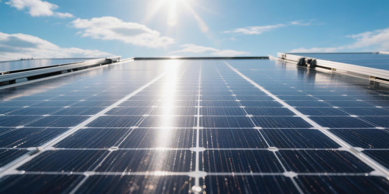
Why Are Monocrystalline Solar Modules So Efficient | Materials, Design, Performance
Monocrystalline silicon purity reaches 99.999%, carrier loss is low;
PERC/TopCon structure elevates efficiency to 22%-24%;
Adopting thin grid lines and anti-reflection coating, lowering resistance and reflectivity to below 2%.
Materials
Purification
Manufacturing high efficiency monocrystalline silicon panels' basic material is high purity polycrystalline silicon material with purity reaching 9N to 11N level. Putting 99.9999999% purity silicon blocks into a quartz crucible and heating to 1420°C's molten state, then through the Czochralski method at a speed of 1 millimeter to 2 millimeters per hour, pulling upwards, single time consuming about 150 hours to grow into a monocrystalline silicon rod with a weight of 300 kilograms to 400 kilograms. Within the crystallization cycle, oxygen atom concentration in silicon liquid is extremely strictly controlled at below 15 parts per million (ppm) per cubic centimeter, and carbon atom concentration must be lower than 1 ppm
Impurity content's variance data is maintained within an extremely small interval, every lowering 0.1 ppm of metal impurity content, finished silicon wafer internal minority carriers' average lifespan can along with it prolong 0.2 milliseconds. Currently, mass-produced N-type crystalline silicon's minority carrier lifespan universally reaches 2 milliseconds to 3 milliseconds range, electrons' degree of freedom moving in the crystal lattice massively rises, physical recombination loss rate dropped about 18%. In material loss's actual statistics, up to 3 meters long silicon rod's two ends have about 15% head and tail defect materials needing to be cut off and returned to the furnace again. The middle 85% qualified segment will then enter the next slice cutting link.
Inside dope a little what
Early period's P-type silicon wafers were mainly doped with boron element, due to the light-induced degradation (LID) phenomenon produced by boron-oxygen complex. Photovoltaic panels under initial 24 hours' outdoor light illumination exposure will produce 2% to 3% power degradation. Current stage's mass production lines have already been large-scale replaced with doping gallium element. Gallium element's segregation coefficient reaches 0.008, not only letting first year light degradation rate plummet to within 0.5% lower limit, but also will modules' linear degradation rate within 25 years life cycle deadly locked at between 0.45% to 0.55% every year.
Occupying current market above 70% share's N-type modules, choose to use phosphorus element as main dopant. Phosphorus atoms' injection amount needs to be precise between 10 to the 15th power to 10 to the 16th power atoms per cubic centimeter, making silicon wafers' base resistivity maintain at 0.3 ohm·centimeter to 1.5 ohm·centimeter standard median value. N-type material structure inherently possesses higher immunity towards metal impurities, dark current density compared to P-type material is lower by a whole order of magnitude, weak light response ability in the morning and evening can extra produce about 4% additional power generation quantity.
Cut thin slices
Monocrystalline silicon rods turning into silicon wafers relies on diamond wire with a thickness of merely 30 micrometers to 36 micrometers conducting high-speed reciprocating physical cutting at 20 meters to 25 meters per second.
· Past's silicon wafer thickness was about 175 micrometers. Currently, P-type silicon wafers' standard thickness has already dropped to 150 micrometers, N-type silicon wafers in batches downward adjusted to 130 micrometers, HJT heterojunction silicon wafers then reached 110 micrometers' extreme physical specifications.
· Thickness every reducing 10 micrometers, every kilogram of silicon block capable of cutting out silicon wafer quantity can increase 6 pieces to 8 pieces, per watt silicon material consumption quantity taking the trend drops to between 2.3 grams to 2.5 grams.
· Kerf physical loss caused by diamond wire cutting is compressed to around 50 micrometers. One piece of square silicon wafer with side length of 182 millimeters or 210 millimeters, after undergoing mechanical polishing and chemical cleaning, surface roughness needs to be controlled within 0.5 micrometers to 1.5 micrometers' error range.
· 110 micrometers silicon wafer's fracture strength test standard needs to be maintained at above 300 megapascals (MPa), production line yield rate is requested to be strictly kept at above 98.5% passing line, any edge micro-cracks or total thickness deviation exceeding 15 micrometers' samples will all be automatically eliminated by high-frequency optical detection equipment.
Silver paste coating
Metallization process collecting silicon wafer surface electrons extremely relies on expensive conductive silver paste materials, silver paste procurement budget occupies the largest material expenditure besides silicon wafers, reaching above 35% of single piece cell's non-silicon cost.
· Silver paste printed on front and back sides is mixed and formed by high purity silver powder with particle size at 1.5 micrometers to 3 micrometers, glass powder, and organic solvent according to 85:5:10's weight percentage.
· Staying 2 seconds to 3 seconds inside an 800°C to 850°C's instantaneous high temperature sintering furnace, silver powder will melt through the surface's silicon nitride anti-reflection layer, forming an ohmic contact with an extremely low resistance value with silicon base.
· Contact resistivity is requested to be smaller than 2 milliohms·per square centimeter, in order to ensure heat conversion loss when current passes through is lowered to a minimum.
· Ordinary P-type cell's single piece silver paste consumption quantity is about 60 milligrams to 75 milligrams, N-type bifacial cell due to front and back both sides all need dense silver grid lines, single piece silver material consumption quantity soars to 100 milligrams to 120 milligrams.
· According to about 1.5 cents to 2 cents per watt's silver paste material cost to calculate, screen printing mesh's opening physical width is shrunk to 13 micrometers to 15 micrometers, printed out silver grid lines' aspect ratio needs to be greater than 0.5, using this while reducing 5% silver material usage amount, to maintain original cross-sectional area and conductive load rate.
Encapsulation film
Photovoltaic modules' outdoor service lifespan is to a huge extent limited by dual-layer encapsulation adhesive film and glass's material physical characteristics.
· Traditional EVA (ethylene-vinyl acetate) adhesive film thickness is usually 0.45 millimeters, light transmittance rate is greater than 91% within the 380 nanometers to 1100 nanometers spectrum range.
· EVA material under double 85 environment test of 85°C environment and 85% relative humidity, water vapor transmission rate is about 20 grams to 30 grams per square meter per day.
· In order to adapt to N-type cells with higher anti-water-vapor requirements, POE (polyolefin elastomer) adhesive film is massively sunken applied. POE's water vapor transmission rate is not up to one tenth of EVA's, merely being 2 grams to 3 grams per square meter per day, volume resistivity is higher by 1 to 2 orders of magnitude.
· Encapsulating silicon wafers and adhesive films together is heat-treated semi-tempered photovoltaic glass with a thickness of 2.0 millimeters. Modules with bifacial double-glass design's total weight is about 27 kilograms to 32 kilograms, load-bearing capacity needs to pass 5400 pascals (Pa)'s front side snow load and 2400 pascals' back side wind load physical test.
· The glass surface is coated with one layer of porous silicon dioxide anti-reflection film with a thickness of 100 nanometers to 150 nanometers, which can reduce light reflectivity of glass and air interface from 4.5% to within 2.0%, making the entire photovoltaic module's actual physical output power increase 2.5% to 3%.
Design
Cut half
Laser equipment at 300 millimeters to 500 millimeters per second moving speed, physically cuts standard square monocrystalline silicon wafer with side length of 182 millimeters or 210 millimeters into two pieces of rectangular half-pieces with equal area. When laser cutting depth reaches one third of the silicon wafer's total thickness, 130 micrometers, which is about 40 micrometers to 50 micrometers, crystalline silicon splitting along the gap's edge roughness is usually controlled within 15 micrometers' physical tolerance interval.
After dividing the whole piece cell into two, the short-circuit current flowing through the single piece cell dropped a full 50% from the original 13 amperes to 18 amperes, lowering to between 6.5 amperes and 9 amperes. According to physics calculation formula, resistance loss is directly proportional to current squared. Nominal current halving makes modules internal electrical energy heat loss ratio massively drop 75%. Under summer 1000 watts per square meter standard sunshine radiation intensity, modules with half-piece design's surface average working temperature is lower than traditional whole piece modules by 1.5 degrees Celsius to 2.5 degrees Celsius.
In partial shadow shading test, when fallen leaves or accumulated dust with area proportion being 15% blocks module bottom, half-piece structure coordinating with 3 bypass diodes with rated current being 20 amperes to 25 amperes, can retain above 50% normal power output, whereas traditional whole piece modules' power loss proportion often is as high as 80% to 100%.
Multiple wires
Regular photovoltaic panels' front side conductive network has already been upgraded from the early period's 5 main grid lines to a dense physical layout scheme of 9 to 18 main grid lines. Circular soldering ribbons with a diameter between 0.22 millimeters and 0.35 millimeters comprehensively replaced past's flat tin-coated copper ribbons with a width of 1 millimeter to 1.5 millimeters, cells' front side metal blocking shadow area shrank from 5% to an extremely low range of 2.5% to 3%.
Due to circular soldering ribbons' arc cross-section possessing optical diffuse reflection characteristics, about 65% to 75% of solar light rays originally shining on soldering ribbon metal surface will be secondarily reflected back to glass and air's interface, thereby with refraction angle lower than 15 degrees shooting into silicon wafer internal again to participate in photoelectric conversion. Physical spacing between adjacent two main grid lines is compressed to between 9 millimeters and 15 millimeters, photo-generated electrons' average physical path moving laterally inside monocrystal to reach collection network shortened by about 30%.
Shortening of transmission distance lowered cell overall series resistance value by 10% to 15%, module's fill factor parameter steadily elevated from 78% to above 82%, single piece photovoltaic panel with an area of 2.58 square meters' total output power therefore increased 5 watts to 10 watts.
Bifacial light transmission
Module backplane material from opaque fluoropolymer thin film with thickness of 0.3 millimeters was replaced with high light transmittance rate semi-tempered glass with thickness of 2.0 millimeters, overall back side light transmittance rate reached above 92% test standard. Bifacial cell's back side adopts partial aluminum back surface field or full coverage's silicon nitride passivation layer physical design, making N-type bifacial module's bifaciality index maintain at 80% to 85% stable interval, while regular P-type module's bifaciality then maintains at 70% to 75% parameter level.
When installed on photovoltaic brackets with height off the ground being 1.0 meters to 1.5 meters, the back side glass can massively absorb reflected radiation from the ground and diffuse reflection light in the natural environment. In ordinary grass fields or dirt environments with surface albedo only being 15% to 20%, bifacial design can produce about 5% to 8% extra power generation quantity gain.
When equipment is deployed on light-colored coated roofs with albedo as high as 60% to 80% or snow-accumulated ground with thickness exceeding 10 centimeters, scattered light absorbed by the back side can push up the system's overall equivalent peak power 15% to 25%, a single piece module with nominal power of 550 watts' actual highest physical output can reach above 680 watts.
Gap becomes gone
Physical spacing between adjacent two pieces of cells internal of monocrystalline modules shrank from the traditional 2-millimeter physical norm to within 0.5 millimeters, high-density products on the market even adopted shingled with negative spacing or flexible conductive adhesive tiling encapsulation technology. Through adopting edge coverage process with physical overlap amount being 1 millimeter to 1.5 millimeters, standard 72 layout photovoltaic panel with dimension of 2278 millimeters by 1134 millimeters' blank inefficient area proportion, was massively compressed from previous 4% to 5% to between 1.5% to 2%.
The elevation of area utilization rate makes photovoltaic modules under physical premise of not increasing even 1 millimeter of length and width size specifications, overall energy conversion efficiency absolute value elevated 0.2% to 0.3%. Conductive adhesive material volume resistivity used in encapsulation process is lower than 0.0005 ohm·centimeter, its curing temperature is precisely set at 150 degrees Celsius to 160 degrees Celsius mild interval, single piece crystalline silicon's mechanical stress release cycle is strictly controlled within 15 minutes to 20 minutes.
Compared to residual thermal stress greater than 50 megapascals produced by traditional high temperature soldering above 260 degrees Celsius, flexible conductive connections lowered the mechanical physical tension borne by silicon wafers by about 60%, after undergoing 200 times of extreme thermal cycle environment tests from minus 40 degrees Celsius to above zero 85 degrees Celsius, module's actual measured power degradation rate is only 1.5%, superior to the 5% performance degradation red line set by the International Electrotechnical Commission.
Performance
Use long time
Photovoltaic panels' rated service age in natural environment is usually set as 25 years to 30 years' long physical cycle. Within this time dimension, N-type monocrystalline modules' first year power degradation rate is strictly limited within the 1.0% upper limit red line, far lower than past polycrystalline products' 2.5% to 3.0% initial degradation amplitude. After entering the 2nd year to 30th year's stable operation period, every year's linear power degradation rate stabilizes at an extremely small fluctuation range between 0.40% to 0.45%.
Assuming one piece of monocrystalline solar panel with an initial nominal power of 600 watts is put into use under standard test conditions (STC), after experiencing up to 360 months of continuous wind blowing and sun scorching, its actual physical output power at the end of the 30th year still is able to maintain between 524.4 watts and 531.6 watts, overall power retention rate is as high as 87.4% to 88.6%. Long-time physical lifespan relies on multiple parameter indicators' collaborative work:
· Encapsulation material water blocking rate: Module water vapor transmission rate is smaller than 2.0 grams per square meter per day, guaranteeing internal cell circuits do not happen electrochemical corrosion under 85% relative humidity.
· Mechanical compression and bending resistance strength: In static mechanical snow load test, bearing 5400 pascals, hidden crack width increment on silicon wafer surface does not exceed 5 micrometers, power loss variance data maintains within 0.3% extremely small deviation degree.
· Ultraviolet exposure tolerance degree: After long-time irradiation through 15 kilowatt-hours per square meter's aging test dosage, surface encapsulation adhesive film's yellowness index (YI) change absolute value is smaller than 1.5, light transmittance rate decline amplitude is merely 0.2%.
· Damp heat extreme test deviation: In up to 1000 hours, 85 degrees Celsius plus 85% humidity's extreme destructive physical test, maximum output power deviation degree is merely 0.8%.
Cloudy days also work
Standard test conditions usually assume sunshine radiation intensity as 1000 watts per square meter, but in actual meteorological distribution statistics, exceeding 45% daytime is situated in weak light environments of cloud layer shading, early morning or evening. The nature of the atomic arrangement inside monocrystalline silicon material makes it within an extremely low weak light interval with radiation intensity being merely 200 watts per square meter, still able to maintain 97% to 98% relative energy conversion efficiency.
When the early morning solar elevation angle is merely 15 degrees, the surface received scattered light illuminance is 150 watts per square meter, and the PN junction internal of the N-type monocrystalline module can then produce 0.5 volts to 0.6 volts open-circuit voltage, early reaching the physical operation working threshold of starting the inverter. Expansion of response spectrum range makes monocrystalline surface coating able to absorb photons with wavelengths situated between 300 nanometers and 1200 nanometers.
Under diffuse reflection spectrum distribution rich in blue light and near ultraviolet light on rainy days, absorbs 4% more photon flux than regular products. Under an environment with illuminance lower than 300 watts per square meter, minority carriers' bulk lifespan maintains at above 1.5 milliseconds, physical recombination rate massively drops 12%.
Installing a 100 kilowatt system within one subtropical monsoon climate region where annual rainfall days reach 120 days, elevation of weak light response ability can let system work 45 minutes early every day and delay shutdown 30 minutes, every year additionally increasing 3500 kilowatt-hours to 4200 kilowatt-hours' effective electrical energy output.
Calculate yield rate
Current market's mainstream high efficiency monocrystalline modules' factory departure unit price is about between 0.12 dollars to 0.15 dollars per watt, initial capital expenditure (CAPEX) is higher than low efficiency modules by about 0.02 dollars per watt. But elevation of conversion absolute value according to equal proportion diluted brackets, cables, inverters as well as land leasing etc. all balance of system (BOS) costs strongly related to area. Single piece monocrystalline module with rated power of 580 watts, its physical dimension is 2278 millimeters by 1134 millimeters, area utilization rate reaches 22.4%.
Evaluate physical and financial parameters | N-type monocrystalline module | P-type monocrystalline module | Polycrystalline module (delisting reference) |
Mass production highest conversion absolute rate | 23.5% | 21.8% | 17.5% |
Nominal power (under same area) | 580 watts | 545 watts | 450 watts |
25 years physical power guarantee rate | 89.4% | 84.8% | 80.2% |
Levelized financial cost of electricity | 0.022 dollars/kilowatt-hour | 0.026 dollars/kilowatt-hour | 0.035 dollars/kilowatt-hour |
Ten thousand kilowatts project BOS total budget | 3.5 million dollars | 3.75 million dollars | 4.3 million dollars |
Project average static payback period | 3.5 years | 4.2 years | 5.8 years |
Laying 1 megawatt's system on commercial real estate roofs, early stage total budget is strictly controlled between 650 thousand dollars and 750 thousand dollars. According to the local power grid standard, every year producing 1.3 million kilowatt-hours of electricity, commercial electricity usage price being 0.18 dollars per kilowatt-hour, every year can save about 234 thousand dollars' electricity bill expenditure. Monocrystalline system's first 5 years' mechanical failure rate and maintenance frequency are extremely low, every year's operation and maintenance fee (OPEX) merely occupies 1% to 1.5% of the total investment amount, namely 6.5 thousand dollars to 11 thousand dollars every year.
Static investment payback time was massively compressed to between 35 months and 42 months. Within the remaining 20 plus years' natural operation cycle, every kilowatt-hour of electricity produced by equipment all represents pure profit value increment. The project's entire life cycle internal rate of return (IRR) statistical distribution usually maintains at 16% to 21% high profitability interval.