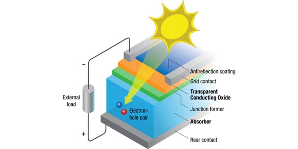
What is a photovoltaic cell and how does it work
Photovoltaic cells directly convert light energy using the photovoltaic effect of semiconductor P-N junctions.
When photons with energy exceeding 1.12 eV excite electron-hole pairs and cause them to move in a directional manner, an electric current is generated.
The Power of the Sun
What exactly is it?
In 2025, global new solar PV installations are expected to exceed 550 GW, a figure reflecting that photovoltaic technology now accounts for over 10% of the total energy mix.
A solar cell is a semiconductor wafer capable of directly converting light energy into electricity, with a base thickness typically maintained between 130 and 150 micrometers.
Each standard-sized 182mm monocrystalline cell can produce a rated power of about 8 to 9 Watts under Standard Test Conditions.
Currently, the energy payback time (EPBT) of mainstream modules on the market is only 0.6 to 1.2 years, meaning they can offset all energy consumed during the production process in approximately one year of operation.
With the iteration of technologies like PERC and TOPCon, the mass-production photoelectric conversion efficiency of individual cells has stabilized in the range of 24.5% to 25.8%, while the cost per Watt has decreased by over 85% in the last 10 years.
What materials are used?
Over 95% of solar products on the market currently use electronic-grade polysilicon as the core raw material, which requires a purity of at least 99.9999999% (9N).
During production, silicon wafers are formed into monocrystalline silicon ingots with diameters of 200 to 300 mm through the Czochralski process, then sliced into 182 mm (M10) or 210 mm (G12) square wafers.
To form the P-N junction required for power generation, boron or phosphorus is doped into the silicon wafer at a concentration of approximately 10^16 atoms per cubic centimeter.
The back of the cell is usually coated with a 10 to 20-micrometer thick aluminum paste layer to form the Back Surface Field (BSF) and improve current collection efficiency.
The cover glass utilizes ultra-white high-transmittance tempered glass with a thickness of 3.2 mm or 2.0 mm, with a transmittance that must exceed 91.5% to minimize light energy loss.
How is electricity generated?
When photons with energy exceeding 1.12 eV strike the surface of the silicon wafer, they excite valence electrons within the silicon atoms, creating freely moving electrons and holes.
Within the depletion region (approximately 1 micrometer wide) inside the P-N junction, a high-intensity built-in electric field exists, driving electrons toward the N-region and holes toward the P-region at a high velocity.
This directional movement of charges generates an open-circuit voltage (Voc) between 0.6V and 0.72V.
Under sufficient light, each square centimeter of the cell surface can generate a short-circuit current density (Jsc) of 38 mA to 42 mA.
Technical Indicator | Parameter Value | Unit |
Silicon Purity | 99.9999999 | % |
Band Gap | 1.12 | eV |
Open-circuit Voltage | 0.68 - 0.72 | V |
Fill Factor | 80 - 85 | % |
Quantum Efficiency | 90 - 95 | % |
What it looks like inside
The top layer of the cell is a silicon nitride (SiNx) anti-reflective coating with a thickness between 70 nm and 100 nm, which reduces the silicon wafer's original reflectance of over 30% to below 5%.
The front surface features 16 to 18 main busbars (Multi-Busbar technology). This MBB design shortens the path of current traveling along fingers, reducing internal resistance loss by approximately 0.5%.
The width of each finger has been thinned from 60 micrometers in the early days to the current 25 to 35 micrometers, increasing the effective light-receiving area by about 1%.
The back of the cell often uses a passivation layer design, utilizing aluminum oxide (Al2O3) or silicon dioxide (SiO2) films to reduce carrier recombination rates at the rear, thereby boosting overall cell efficiency by 0.5% to 1%.
How to distinguish quality
The core indicator for measuring cell performance is conversion efficiency.
Currently, the efficiency limit for P-type PERC cells is around 24.5%, while the mass-production efficiency of N-type TOPCon cells has exceeded 26%.
Besides efficiency, the temperature coefficient is a key metric. Standard monocrystalline silicon cells have a temperature coefficient of approximately -0.3% to -0.35% per degree Celsius; for every 10°C rise in ambient temperature, the power generation drops by about 3% to 3.5%.
Over a 25-year service life, the total power degradation should be controlled within 15%, with the initial degradation in the first year typically being less than 1% to 2%.
Rear-side generation gain of bifacial cells is also an evaluation point. Depending on the ground reflection environment, the rear side can contribute 5% to 25% additional power output.
How much power can it generate?
A residential PV system with an installed capacity of 10 kW in a region with an average of 4 hours of equivalent peak sunshine per day has an annual power generation of approximately 14,000 to 15,000 kWh.
Considering inverter conversion efficiency (approx. 98%), cable losses (approx. 1% to 2%), and losses caused by dust accumulation on the module surface (approx. 3% to 5%), the overall Performance Ratio (PR) of the system usually operates between 75% and 85%.
Each square meter of a PV array can produce 200 to 220 Watts of power per hour on average; installing a 1KW system requires approximately 5 to 6 square meters of roof area.
Based on the current module price of $0.12 per Watt, the hardware cost of the entire system is about $1,200.
Combined with a local electricity price of around $0.1 per kWh, the static investment payback period is typically between 4.5 and 6 years.
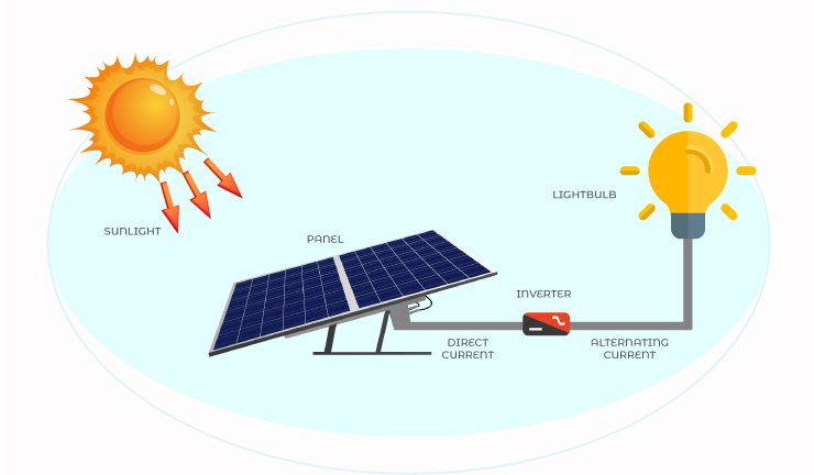
How It Works
Light-to-electricity process
Photons in sunlight with wavelengths between 300 nm and 1200 nm carry different levels of energy.
When photons with energy greater than 1.12 eV enter a 140-micrometer thick silicon wafer, they excite free electrons and holes within a surface layer of 2 micrometers in depth.
This energy conversion process is limited by the Shockley-Queisser limit, which locks the theoretical conversion upper limit of single-junction crystalline silicon cells at around 33.7%.
Under standard irradiance of 1,000 W/m², each square centimeter of light-receiving area can generate approximately 40 mA of short-circuit current.
This physical induction effect can be completed within 1 nanosecond, ensuring the immediacy of energy conversion.
Energy excitation requires only 1.12 eV.
Wavelength coverage: 300 to 1200 nm.
Response speed reaches nanosecond level.
Inside the silicon wafer
Mass-produced 182mm cells mainly adopt a P-N junction structure, achieved by doping different elements into silicon crystals with a purity of 99.9999999% (9N).
The N-type region is doped with phosphorus atoms at a concentration of 10^19 per cubic centimeter through a diffusion process, while the P-type substrate contains boron atoms at a concentration of approximately 10^16 per cubic centimeter.
The built-in electric field formed at the interface of the two layers is about 0.5 micrometers thick, with a barrier height usually between 0.6 V and 0.7 V.
To increase the light-receiving area, the silicon wafer surface utilizes chemical etching to create pyramid-shaped textures (texturing) with a height of about 3 to 5 micrometers.
This structure allows incident light to undergo 2 to 3 reflections on the surface, forcibly reducing the original silicon wafer's 35% reflectance to below 10%.
Silicon purity reaches 9N level.
Texture height: 3 to 5 micrometers.
Reflectance reduced from 35% to 10%.
How electrons escape
Under the influence of the P-N junction's built-in electric field, light-excited free electrons drift toward the light-receiving surface at a speed of 10^5 meters per second.
In high-quality silicon wafers with diffusion lengths reaching 200 to 300 micrometers, electrons can survive for 100 to 1,000 microseconds before recombination.
This time span is sufficient for charges to pass through the 140-micrometer thick substrate to reach the electrodes.
If the impurity content inside the silicon wafer exceeds 10^12 atoms per cubic centimeter, the electron recombination rate will rise by over 15%.
The open-circuit voltage of the cell is significantly affected by temperature; typically, for every 1°C increase in temperature, the voltage drops by 2.2 millivolts.
To suppress this thermal loss, modern cell processes stabilize the voltage at operating temperatures within the range of 0.68V to 0.72V.
Drift speed: 100,000 meters per second.
Electron lifetime up to 1000 microseconds.
Voltage drops 2.2 mV per degree.
Extracting the current
16 to 18 main busbars with a width of approximately 0.1 mm are distributed on the front of the cell to collect current from the fingers.
Finger width has currently been optimized to 25 to 35 micrometers to reduce shading loss by about 1.5%.
These electrodes are usually made of conductive silver paste with a silver content of over 90% via screen printing, with silver consumption per cell controlled between 80 mg and 100 mg.
To reduce ohmic losses, the contact resistance must be pushed down to below 3 milliohms per square centimeter.
By increasing the number of busbars, the current collection path is shortened by over 25%, which improves the cell's fill factor to a level of 82% to 85%.
Number of busbars: 16 to 18.
Silver consumption below 100 mg.
Fill factor reaches over 82%.
Where does efficiency go?
PV modules encounter various energy losses during operation, with about 20% of incident energy being converted into heat due to non-absorption of long-wavelength light.
The silicon nitride thin film (70-90 nm thick) covering the surface is primarily used to reduce the surface recombination rate of carriers.
Currently, the average mass-production efficiency of TOPCon cells remains between 25% and 26%, while rear-side generation gain can provide an additional 5% to 15% output.
Because the POE or EVA encapsulant used for module packaging has a light transmittance of around 90%, the actual efficiency after assembly is about 1% lower than that of individual cells.
Over a 25-year lifecycle, UV radiation and thermal stress cause a linear power degradation of 0.4% to 0.55% per year.
Thermal loss accounts for 20%.
Passivation film thickness: approx. 80 nm.
Annual degradation rate below 0.55%.
Lifespan coverage
The design service life of industrial-grade PV systems is typically set at 30 years, requiring that total power generation during this period remains at least 80% of its initial value.
Cells are encapsulated in a 2.0 mm thick double-glass structure to resist snow loads of up to 2400 Pa or wind loads of 5400 Pa.
Internal bus ribbons use 0.2 mm thick tin-coated copper ribbons, with power loss caused by connection resistance controlled within 0.5%.
As auxiliary equipment, the Maximum Power Point Tracking (MPPT) efficiency of the inverter is usually as high as 99.5%.
With a comprehensive system loss of 15%, a 100KW distributed system can generate approximately 130,000 to 150,000 kWh of energy annually, equivalent to an installation cost of about $0.25 to $0.35 per Watt.
Key Concerns
Heat sensitivity
PV cells exhibit extreme sensitivity to ambient temperature; the 25°C set for standard test conditions differs greatly from the actual outdoor operating environment.
When the module surface temperature rises from 25°C to 65°C, the output power of P-type monocrystalline silicon modules decreases linearly at a coefficient of -0.35% per degree.
In the hot summer, the actual output of the module can lose about 14% of its original rated power.
Voltage drop is the main incentive for this efficiency loss; the open-circuit voltage decreases by approximately 2.2 millivolts per degree rise.
To mitigate thermal loss, installation racking must reserve a 10 to 15 cm ventilation gap, using air convection to lower the module's backsheet temperature by 5 to 8 degrees.
In regions where ambient temperatures exceed 40°C, choosing N-type cells with a lower temperature coefficient (e.g., -0.3% per degree) can increase annual power generation by about 3.5%.
Temperature Indicator | Parameter Impact | Value Reference |
Standard Test Temp | Rated power baseline | 25°C |
Power Temp Coeff | Efficiency drop rate | -0.3% to -0.39% / °C |
Voltage/Temp Variation | Open-circuit voltage drop | 2.2 mV / °C |
Recommended Gap | Ventilation/cooling needs | 10 to 15 cm |
Slower degradation
Modules typically undergo Light Induced Degradation (LID) in the first year after commissioning, leading to a power drop of 1.5% to 2% within the first 100 hours.
Throughout a 30-year total service cycle, the linear degradation rate must be strictly controlled between 0.45% and 0.55% per year to ensure residual power at the end of the term is at least 80% of its initial value.
If excess moisture is introduced during the encapsulation process, the internal ethylene-vinyl acetate (EVA) film will undergo a hydrolysis reaction.
This reaction produces acetic acid at concentrations exceeding 100 ppm, corroding the internal metal fingers and triggering Potential Induced Degradation (PID).
Power plants affected by this may see serious consequences, such as a sudden drop in output of over 30% after 3 years of operation.
High-quality modules have increased the guaranteed residual power after 25 years to over 87% by optimizing the passivation layer process.
Each 182 mm cell is expected to generate approximately 450 to 550 kWh of energy over its full lifecycle.
First-year LID rate: 1.5% to 2.0%.
30-year life: Power must remain above 80%.
Encapsulant acetic acid: <100 ppm to prevent corrosion.
Shading issues
Even if partial shading covers only 3% of the panel surface, it can cause the current output of the entire module string to drop by more than 25% due to the hot spot effect.
When a single cell is shaded by tree shadows, wires, or bird droppings, it transforms from a power source into a power-consuming resistor, and the local temperature can soar to over 100°C within 10 seconds.
To protect the circuit from being burnt by high temperatures, three bypass diodes are usually configured in the junction box, which automatically cut off affected sections when the current difference exceeds 10%.
Although this protection mechanism avoids fire risk, it causes the system voltage to instantly drop by one-third, which in turn affects the inverter's tracking efficiency.
In distributed rooftop systems, installing power optimizers can recover about 15% to 20% of the energy loss caused by shading.
Cost calculation
Currently, the Levelized Cost of Energy (LCOE) for global PV systems has dropped to $0.03 to $0.05 per kWh in sunlight-rich regions.
Module procurement costs account for only about 40% of the initial capital expenditure (CAPEX) of the total system, with the remaining 60% allocated to racking, cables, inverters, and labor.
The design life of an inverter is typically 10 to 12 years, meaning that during the 30-year operation period, funds amounting to about 10% of the initial investment should be reserved for two equipment replacements.
Operation and maintenance (OPEX) costs are approximately $10 to $15 per kW per year, covering cleaning, inspections, and insurance.
If the loan interest rate remains below 5% and the local average electricity price is higher than $0.1, the static investment payback period of the project can usually be locked in between 5.5 and 7.2 years.
Cost Item | Proportion | Value Reference (USD) |
Module Procurement | Total CAPEX | Approx. 40% |
Inverter Lifespan | Operating Cycle | 10 to 12 Years |
Annual O&M Cost | Per kW Cost | $10 to $15 |
Payback Period | Profit Turning Point | 5.5 to 7.2 Years |
Soiling loss
The impact of surface dust accumulation on power generation varies with geographical environments; soiling loss in arid and windy regions can reach 5% to 15% per month.
When dust accumulation reaches 10 grams per square meter, transmittance drops by approximately 4.5%, leading to a reduction in daily equivalent generation time by 20 to 40 minutes.
The cost of manual cleaning using deionized water is approximately $0.5 per square meter; although frequent cleaning can yield a 3% power generation gain, water fees and labor expenses must be balanced.
For bifacial modules, the ground reflection light received by the rear side can provide an additional 10% to 25% power gain.
This requires the module installation height from the ground to be maintained at 1 meter or more, and the ground albedo (such as white gravel or snow) must be higher than 30% to achieve maximum efficacy.
End-of-life disposal
By 2030, the total weight of retired PV modules globally is expected to exceed 8 million tons, making recycling a significant item on the environmental bill.
A standard-sized module weighs about 19 kg, of which the aluminum alloy frame accounts for 18% and the cover glass accounts for 65% to 75%.
Through physical crushing and thermal treatment processes, more than 90% of the glass and aluminum, as well as recycled silicon with a purity of 99%, can be recovered.
The current recovery value of silver is approximately $600 to $800 per kilogram.
Although the silver content per cell is only about 0.1 gram, the economic return remains considerable in the decommissioning of MW-scale power plants.
Establishing a sound circular mechanism can reduce the carbon footprint per Watt of modules by 25%, ensuring that the PV industry complies with carbon emission requirements of international green trade policies.