How To Generate Electricity From Solar Panels | 3 Steps
Three-step power generation: First, use monocrystalline silicon panels with an efficiency of about 20% to capture sunlight and convert it into DC power;
Second, convert it into 220V AC power through an inverter for household appliances;
Finally, excess power can be connected to the grid or stored. Professional installation usually saves families about 30% on electricity bills, making it both efficient and reliable.

Absorption
How Much Light is Absorbed
The energy density of solar radiation reaching the Earth's surface is 1,000 W/㎡ under standard conditions, but silicon-based photovoltaic cells cannot absorb all the energy.
The bandgap of crystalline silicon is 1.12 eV, which means only photons with wavelengths shorter than 1100 nm can be effectively absorbed to excite electron-hole pairs.
In the entire solar spectrum, about 25% of the energy is in the infrared band, which is lost by penetrating the silicon wafer because the energy is lower than 1.12 eV.
Current mainstream N-type TOPCon cells can increase the short-circuit current (Isc) density to over 42 mA/cm² by optimizing the thin-film structure.
Under AM1.5 spectral conditions, the absorption rate of 150-micron thick monocrystalline silicon wafers for the 400 nm to 1000 nm band has reached over 95%.
Parameter Item | Detailed Value | Impact on Efficiency |
Spectral Absorption Range | 300nm - 1100nm | Determines the theoretical conversion efficiency upper limit of 29.4% |
Silicon Bandgap | 1.12 eV | Photons below this energy provide 0 power contribution |
Energy Loss Ratio | About 23% - 25% | Mainly penetration loss of long-wave infrared rays |
Carrier Generation Rate | 10^17 per second per square centimeter | Determines the basic strength of the cell's output current |
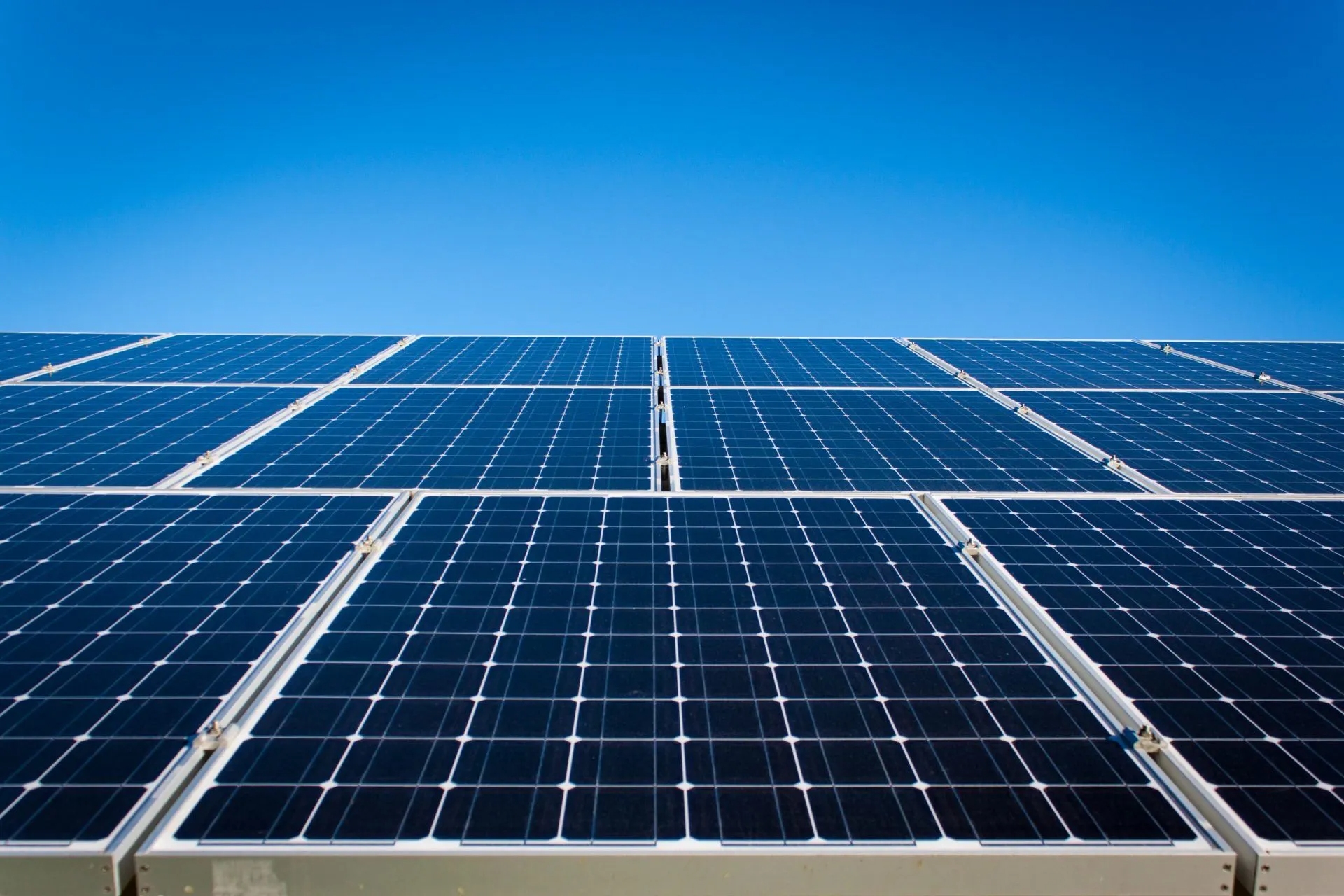
Non-reflective surface
The surface of a bare silicon wafer acts like a mirror, reflecting about 35% of the incident light, which leads to a significant drop in power generation efficiency.
To solve this problem, manufacturers create a pyramid-shaped textured structure with a height between 3 to 5 microns on the silicon wafer surface through an alkali etching process.
This structure allows light to undergo multiple reflections on the surface, reducing the initial reflectivity from 35% to about 10%.
Subsequently, a silicon nitride (SiNx) anti-reflection film with a thickness of about 70 to 80 nanometers is deposited on the cell surface, further controlling the reflectivity below 2% using the principle of thin-film interference.
The refractive index of this film is usually set at around 2.0, perfectly matching air (refractive index 1.0) and silicon (refractive index 3.4).
Surface Process | Reflectivity Change | Technical Detail Indicators |
Polished Silicon Wafer | 30% - 35% | Belongs to the raw state without processing |
Textured Pyramid | 10% - 12% | Structure base width is usually 2 - 4 microns |
Silicon Nitride Coating | 1.5% - 2% | Coating thickness error must be controlled within ±3 nm |
Total Light Capture Rate | Over 98% | Ensures that over 980 W of light energy per kilowatt enters the cell |
Silicon Wafer Thickness
Mainstream silicon wafer thickness in the market has been reduced from 180 microns to 150 microns, and some high-efficiency N-type cells have even begun to try 130-micron processes.
Although thinning the silicon wafer can save more than 15% in material costs, if it is too thin, it will affect the absorption capacity for long-wave light.
Experimental data shows that 90% of high-energy short-wave light is absorbed within the first 10 microns of depth in the silicon wafer, but long-wave light above 900 nm requires a path of more than 100 microns to be fully captured.
To compensate for the absorption loss caused by thinning, an aluminum oxide (Al2O3) passivation layer is added to the back of the cell, forming a mirror-like internal reflection effect that reflects penetrating light back into the interior for re-absorption.
Specification Parameters | Specific Value | Economic and Performance Logic |
Mainstream Wafer Thickness | 150 - 155 μm | Reduces cost by about 0.1 yuan/piece compared to 180 μm |
Long-wave Absorption Depth | Above 100 μm | Determines that the back reflection layer must have 95% reflectivity |
Back Passivation Layer | 10 - 20 nm | Increases internal reflectivity, adding 0.5% absolute efficiency |
Silicon Wafer Breakage Rate | Below 0.3% | Requires higher-strength brackets when thickness is reduced to 130 μm |
Heat Loss
The process of absorbing light energy is accompanied by intense thermal effects; the portion of photon energy exceeding 1.12 eV is converted into heat.
This thermalization loss accounts for about 33% of the total incident energy, causing the module temperature to rise to 60 degrees Celsius under summer exposure.
For common monocrystalline silicon modules, for every 1 degree increase in temperature, the power generation will drop by 0.3% to 0.35%.
If the module operating temperature rises from the standard laboratory temperature of 25 degrees to an actual operating temperature of 45 degrees, the total output power will evaporate by 6% to 7%.
Therefore, while absorbing light, high-efficiency cells must rely on high heat dissipation coefficients (usually required to be above 2.0 W/m·K) from aluminum frames and backsheets to forcibly cool down.
Loss Item | Ratio/Coefficient | Actual Operating Impact |
Thermalization Loss Ratio | About 33% | Causes module surface temperature to be 20 - 30 degrees higher than ambient |
Power Temp Coefficient | -0.34% / ℃ | For every 10 degree rise, a 10 kW system generates 340 watts less electricity |
Operating Temp (NOCT) | 45 ± 2 ℃ | Measures the thermal balance capability of the system under natural ventilation |
Dissipation Backsheet Thickness | 300 - 350 μm | Determines the speed at which internal heat is conducted to the air |
Charge Carrier Lifetime
Electrons generated after photons are absorbed must flow to the electrodes before being recombined; otherwise, energy will dissipate as fluorescence or heat.
In N-type cells, the minority carrier lifetime can reach over 3 milliseconds, far higher than the 1 millisecond of P-type cells.
This means electrons migrate longer distances internally, with a higher probability of collection.
If the impurity concentration inside the silicon wafer exceeds 10^12 atoms/cm³, or if surface passivation is uneven, electrons will recombine within 10 microseconds, causing the open-circuit voltage (Voc) to drop from an ideal 730 mV to 680 mV or even lower.
Current advanced cell processes require a silver content in the paste of over 90% to ensure extremely low contact resistance, allowing the converted current to enter the external circuit with a 99% collection rate.
Physical Indicators | Target Value | Technical Output Result |
Carrier Lifetime | 3000 - 5000 μs | Supports cell conversion efficiency breaking through 25.5% |
Surface Recombination Velocity | < 10 cm/s | Ensures open-circuit voltage (Voc) stays above 720 mV |
Contact Resistance | < 1.0 mΩ·cm² | Reduces the final 1% loss of power at the output port |
Fill Factor (FF) | 82% - 85% | Reflects the final utilization quality of absorbed energy by the cell |
Conversion
How Electricity is Generated
When photons with energy exceeding 1.12 eV hit the P-N junction inside the silicon wafer, electron-hole pairs are excited within 10 nanoseconds.
In a 150-micron thick monocrystalline silicon wafer, the boron doping concentration in the P-type region is usually maintained at 10^16 atoms/cm³, while the phosphorus diffusion depth in the N-type region is precisely controlled between 0.3 to 0.5 microns, thereby establishing an internal electric field of about 0.7 volts.
This electric field provides the driving force for directional movement of carriers, causing photogenerated electrons to enrich toward the N region at speeds of several kilometers per second.
Current mainstream N-type cells, due to their substrate material resistivity distributed between 0.5 to 1.5 Ω·cm, can support higher carrier mobility, increasing the open-circuit voltage (Voc) of a single cell from 680 mV in traditional processes to over 730 mV.
· Internal Potential Height: 0.7V - 0.75V
· Diffusion Layer Thickness: 300 nm - 500 nm
· Substrate Resistivity: 0.5 - 1.5 Ω·cm
· Open-circuit Voltage Performance: 710mV - 745mV
Where Efficiency is Limited
The theoretical upper limit of converting light energy into electrical energy is determined by the Shockley-Queisser limit, which is approximately 29.4% for single-junction crystalline silicon cells.
In actual production, the conversion efficiency of currently mass-produced TOPCon cells is distributed between 25.5% and 26.3%, while the laboratory efficiency of Heterojunction (HJT) cells has exceeded 27.5%.
Main efficiency losses stem from the penetration loss of long-wave infrared light, accounting for about 20% of the total energy, and the thermalization loss of high-energy photons, accounting for more than 30%.
To approach the theoretical limit, manufacturers deposit an ultra-thin silicon dioxide tunneling layer with a thickness of 1 to 2 nanometers on the back of the cell, combined with a 150-nanometer thick doped polysilicon layer. This passivated contact structure can reduce the surface recombination velocity to below 5 cm/s, increasing the absolute conversion efficiency by 1.5% to 2.0%.
· Theoretical Conversion Limit: 29.4%
· Mass Production Average Efficiency: 25.8%
· Tunneling Layer Thickness: 1.2 nm - 1.8 nm
· Surface Recombination Velocity: < 5 cm/s
How Current Flows
Excited electrons must pass through a complex grid line network to enter the external circuit. This process generates series resistance (Rs) that must be kept below 0.25 Ω·cm².
Currently, the surface of 182mm specification cells is usually covered with 16 to 18 main busbars, with the width of each busbar reduced from 0.1mm to 0.03mm to reduce the shading area by about 2%.
To reduce ohmic losses, the silver content ratio in the paste should reach 85% to 90%, ensuring the short-circuit current (Isc) of a single cell reaches 13.5A to 14.2A.
If contact resistance exceeds 1.5 mΩ·cm², energy loss at the interface converts into heat, causing local module temperature to rise by 3 to 5 degrees Celsius within 1 minute, which in turn drops the Fill Factor (FF) of the entire string from an ideal 83% to below 78%.
· Series Resistance Index: < 0.3 Ω·cm²
· Number of Busbars: 16BB - 20BB
· Single Cell Current Intensity: 13.5A - 14.5A
· Fill Factor Range: 80% - 85%
How Much Loss
Physical losses are inevitable during the conversion process, where the size of the leakage current (Shunt resistance) is the measure of cell quality.
The shunt resistance (Rsh) of high-performance cells should be greater than 5000 Ω·cm². If metal impurities exist internally, leakage current will cause microvolt-level fluctuations in output voltage every second.
At the same time, for every 1 degree Celsius increase in temperature, the bandgap of the silicon wafer narrows, causing the voltage output to drop by about 0.3% / ℃.
This means that under conditions where the ambient temperature is 35 degrees Celsius and the module backsheet temperature reaches 65 degrees, a 25.5% efficiency cell will actually have an operating efficiency drop to around 22.5%.
Additionally, due to Light-Induced Degradation (LID), P-type cells have a power loss of about 2% in the first year, while N-type cells can control this figure within 1%, ensuring that the total output power after 25 years remains between 87.4% and 89.5% of the initial value.
· Shunt Resistance Requirement: > 5000 Ω·cm²
· Temperature Influence Coefficient: -0.29% / ℃ to -0.34% / ℃
· First Year Degradation Rate: 0.4% - 1.0%
· 25-year Power Warranty: > 87.4%
More Efficient Collection
By coating the back of the silicon wafer with a 20-nanometer thick aluminum oxide film, a strong field passivation effect can be generated, reflecting holes from the back to the substrate and increasing the Internal Quantum Efficiency (IQE) by more than 10% in the 900 nm to 1100 nm long-wave band.
This process upgrades single-sided cells to bifacial cells. The back gain rate usually fluctuates between 5% and 25%, depending on the ground reflectivity (grass reflectivity is about 15%, while white-painted ground can reach 80%).
In a 10 kW distributed system, using these high bifaciality modules (bifacial ratio over 80%) can generate an additional 2 to 4 kWh of electricity per day, which corresponds to a 10 to 14 month reduction in the entire investment recovery period, lowering the Levelized Cost of Electricity (LCOE) by about 0.03 yuan per watt.
· Back Passivation Thickness: 15nm - 25nm
· Internal Quantum Efficiency: > 95% (Short and medium wave)
· Back Gain Range: 10% - 25%
· LCOE Reduction: 0.02 - 0.05 yuan/kWh
Distribution
How Power is Distributed
The 230V or 400V AC output from the inverter side first needs to be initially integrated through an AC combiner box.
For a three-phase system with a rated power of 10 kW, its full-load output current is about 14.5 A, while the current of a single-phase system will soar to over 43.5 A.
To ensure the stability of power distribution, the temperature rise of the busbars inside the distribution box must be controlled within 30 degrees Celsius, and the rated current of a single branch must be redundantly designed according to 1.25 times the maximum current of the system.
In actual operation, the output terminal voltage of the inverter will be 2V to 5V higher than the grid side. This tiny pressure difference ensures that photovoltaic power is prioritized for consumption by household loads with 99% priority, rather than flowing directly to the grid.
Distribution Link Parameter | Standard Quantitative Index | Performance Impact Factor |
Rated Output Voltage | 230V (Single-phase) / 400V (Three-phase) | Allowed fluctuation range is ±10% |
Max Output Current | 14.5A - 45.0A | Determines the rated current choice for circuit breakers |
Distribution Frequency Precision | 50 Hz ± 0.1 Hz | Frequency shift over 0.2 Hz triggers grid disconnection protection |
Total Harmonic Distortion (THD) | < 3.0% | Protects the operating life of precision electronic equipment |
Wires Must Be Thick Enough
Under 1000 watts of transmission power, if a 2.5 mm² copper core wire is used for 20 meters, its voltage drop might reach 2.5%. This not only wastes about 25 watts of power but also causes the inverter to frequently report errors due to perceiving excessively high terminal voltage.
Industry standards require the AC side voltage drop to be controlled within 1%. Therefore, for wiring distances over 15 meters, the use of 6 mm² or 10 mm² national standard copper cables is usually mandatory.
The resistivity of copper cable at 20 degrees Celsius is about 0.0172 Ω·mm²/m, which means for every 10 meters of wiring added, the loop resistance increases by about 0.034 ohms. For systems running at high currents, this generates more than 50 watts of heat dissipation per hour.
The insulation class of the cable must reach over 1000 V and possess UV resistance, ensuring continuous operation for 25 years at an outdoor high temperature of 60 degrees Celsius without embrittlement.
To prevent current from arcing at joints, the contact resistance of all crimp terminals should be lower than 0.5 milliohms.
During installation, the bending radius of the cable must not be less than 6 times the cable diameter to prevent internal copper wires from breaking under stress.
After four hours of high-load operation, the actual surface temperature of the cable should not exceed the ambient temperature by more than 20 degrees Celsius; otherwise, the wire gauge must be upgraded or ventilation improved to maintain system transmission efficiency above 98.5%.
Cable Spec (Copper Core) | Rated Ampacity (30℃) | Voltage Drop at 20 m (40 A) | Loss Power (Watts) |
4 mm² | 32 A | 3.4% (Approx 7.8 V) | 312 W |
6 mm² | 42 A | 2.2% (Approx 5.1 V) | 204 W |
10 mm² | 56 A | 1.3% (Approx 3.0 V) | 120 W |
16 mm² | 75 A | 0.8% (Approx 1.8 V) | 72 W |
Guard the Gateway
The safety modules inside the distribution box are the physical barriers of the entire distribution system. The rated breaking capacity of the AC circuit breaker (MCB) must reach 6kA or 10kA to ensure current is quickly cut off within 0.01 seconds in the event of a short circuit fault.
To prevent tiny leakages from harming humans, the system must be equipped with a Type B Residual Current Device (RCD), with the leakage action current set at 30 mA and the action time less than 0.1 seconds.
Additionally, the discharge current of the Surge Protective Device (SPD) must reach 20kA to 40kA, capable of diverting instantaneous overvoltage to below 1.5 kV within microseconds of an induced lightning strike, protecting the power modules inside the inverter, which are worth thousands of yuan, from breakdown.
The protection level of the distribution box should reach IP65, which means it can completely prevent dust entry and withstand water jets of 12.5 liters/minute.
The spacing of the internal wiring rows should be maintained at more than 12 millimeters to prevent creepage in high humidity environments.
During installation, the torque of every screw needs to be calibrated using a torque wrench between 2.5 N·m and 4.0 N·m, preventing poor contact caused by long-term vibration.
Statistics show that increased local contact resistance due to loose wiring can cause node temperatures to rise to 200 degrees Celsius within 10 minutes, becoming the cause of 80% of fire hazards in photovoltaic systems.
Grid Connection Accounting
The final step in power distribution is connecting to the public grid.
This requires installing a bidirectional smart meter, which can record the electricity consumed by the family and the surplus electricity fed back to the grid in 15-minute collection cycles.
To ensure grid quality, the power factor (PF) of the system should be maintained between 0.95 and 1.0. If the power factor is lower than 0.9, the grid company may require the installation of reactive power compensation devices.
When the grid loses power due to a fault, the anti-islanding protection within the distribution system must cut off the output within 2 seconds to prevent the system from feeding power back to the grid, ensuring no dangerous voltage exists within the working radius of line maintenance personnel.
Monitoring Index | Ideal Numerical Range | Abnormal Consequence |
Bidirectional Meter Accuracy | 0.5S class or above | Settlement income generates 1% - 3% deviation |
Power Factor (PF) | 0.98 - 1.00 | Below 0.9 may result in fines |
Islanding Protection Response | < 2.0 seconds | Causes electric shock risk for grid maintenance personnel |
Grid Connection Point Voltage Fluctuation | < 7% of rated value | Causes household appliances to fail to start or burn out |
Stored for Backup
Hybrid inverters need to complete the switch from grid-connected mode to off-grid mode within 20 milliseconds, which is fast enough to ensure that devices like computers and routers do not restart during a power outage.
The DC cables on the cell side usually need to carry high currents of over 100 A, so dedicated flexible cables of 25 mm² or 35 mm² must be used.
In the power distribution strategy, the system will adjust in real-time based on the State of Charge (SOC) of the cell. When the SOC is lower than 20%, power supply is stopped to protect the lifespan, and when the SOC reaches 100%, surplus electricity is fully directed to the AC side loads, achieving 100% energy utilization.