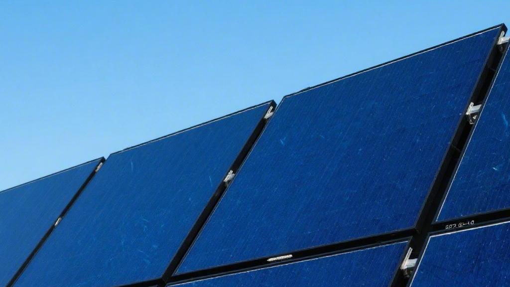
What are the latest innovations in monocrystalline solar module technology?
The latest monocrystalline silicon technology focuses on N-type TOPCon and Heterojunction (HJT), with conversion efficiencies exceeding 25% and first-year degradation below 1%.
It is recommended to purchase bifacial N-type modules and lay white gravel on the installation ground to increase reflectivity. Utilizing backside power generation can yield an additional 10% to 30% in actual returns.

TOPCon and HJTB
Competing on Bifaciality
In the first quarter of 2026, the total commissioned production capacity of N-type cell lines on the global market broke through the 450 gigawatt (GW) threshold. The peak conversion rate of single-sided light-receiving panels from the previous era stalled at the physical bottleneck of 24.5% in laboratory tests.
After transitioning to the bifacial absorption mechanism, the photoelectric absorption and conversion ratio on the back of TOPCon modules jumped significantly to a parameter range of 80% to 85%. Due to its symmetrical structural and physical characteristics, another route, HJT, pushed the bifacial absorption rate to the extreme band between 92% and 95%.
l In a standard sandy environment with a 30% albedo, a 1-megawatt HJT array can generate approximately 4,500 kilowatt-hours of additional electricity per month.
l If a white polymer reflective film with a reflectivity as high as 75% is laid on the ground, the annual average equivalent full-load utilization hours of a 100-megawatt power plant will climb from 1,600 hours to around 1,850 hours.
l The Levelized Cost of Energy (LCOE) amortized over the entire system lifecycle decreases by about 4.5% to 5.2% alongside this 250-hour additional power generation increment.
Ultra-Thin Oxide Layer
The retrofitting cost for the world's top five manufacturers to upgrade their legacy production lines to TOPCon lines is approximately $0.015 to $0.02 per watt.
Automated production equipment precisely deposits a silicon dioxide thin film with a thickness of only 1.2 to 2.0 nanometers on the back of the N-type silicon wafer. On top of this extremely thin separator, another microscopic capping layer of doped polycrystalline silicon, about 15 to 20 nanometers thick, is superimposed.
The quantum tunneling effect in physics gives electrons a 99.9% success rate in passing through this 1.5-nanometer gap, while the blocking and interception rate for hole atoms is maintained above 99.2%. The one-way transmission mechanism for specific electrons reduces the recombination current density in the metal contact area to below 10 femtoamperes per square centimeter (fA/cm²).
l By eliminating high-recombination region losses, the open-circuit voltage parameters at both ends of the cell are easily elevated into a stable operating range of 720 millivolts to 730 millivolts.
l Under Large-Scale Standard Test Conditions (STC) at 25 degrees Celsius, the average mass-production conversion efficiency of individual cells coming off the line stabilizes within a narrow distribution band of 25.8% to 26.2%.
l For a finished silicon wafer measuring 182 mm by 182 mm, its terminal output power is about 1.2 to 1.5 watts higher than that of the previous generation of products.
Amorphous Silicon Film
The entire silicon wafer processing workflow for HJT contains only 4 main independent process steps, reducing the machine transfer and handling time by nearly 60% compared to TOPCon's 9 to 11 routing steps.
The maximum heating and processing temperature in the manufacturing workshop is strictly controlled to operate between 200 degrees Celsius and 250 degrees Celsius. By replacing the traditional high-temperature sintering furnaces (which operated above 850 degrees Celsius) with a 200-degree low-temperature process, the factory manufacturing power consumption for a single cell drops significantly by about 35.4%.
Both the front and back sides of the roughly 130-micrometer-thick N-type silicon baseplate are individually coated with an intrinsic amorphous silicon layer ranging from 5 to 10 nanometers in thickness.
l Relying on the extremely high surface and interface passivation performance parameters of the amorphous silicon material, the open-circuit voltage reading on the tester can stably break through the 750-millivolt mark and even approach the high threshold of 760 millivolts.
l Sample inspection data from 100,000 pieces in the fourth quarter of 2025 showed that the average photoelectric efficiency of batch-produced HJT cells reached the mass-production milestone of 26.5%.
l The defective rate on the production line is compressed to between 0.8% and 1.2%, reducing the hidden manufacturing cost of $0.005 per watt caused by recycling and remelting discarded silicon wafers.
IBC and XBC
All-Black Front
In the high-end residential rooftop markets of North America and Europe in 2026, XBC (Interdigitated Back Contact and its derivative architectures) modules secured an extremely high procurement share. The visual surface of a standard 2-square-meter panel completely eliminates the 0.2 mm to 0.3 mm wide silver busbars. Removing the physical obstruction of metal wires frees up 3.5% to 5.2% of pure light-receiving area for the front optical absorption layer.
Photons hitting the anti-reflective coating enter the silicon wafer unhindered with a 99.8% penetration rate. The short-circuit current density parameter on measuring instruments jumps from 40.5 milliamperes per square centimeter for traditional panels to over 42.8 milliamperes. By eliminating the shading losses caused by silver paste, the conversion rate of monocrystalline cells outputted from laboratory test ports touches the extreme value of 27.1%, while the average parameters of finished cell strings coming off mass-production assembly lines also maintain a high operating range of 26.4% to 26.6%.
In independent third-party testing laboratories in Munich and California, an all-black XBC module with an area of 2.58 square meters achieved an actual peak output power of 635 to 650 watts under Standard Test Conditions (1000 watts/square meter, 25 degrees Celsius).
Backside Routing
The entire processing technique transfers all positive and negative electrical contact points entirely to the dark rear side of the 130-micrometer-thick N-type silicon wafer. The P-type and N-type doped regions are designed as alternating, parallel zebra-stripe patterns, typically requiring extremely precise machine laser alignment and engraving at the 15- to 20-micrometer level.
Electron-hole pairs excited by light near the front surface layer must traverse a full depth of 130 micrometers to reach the metal contact channels on the back. To ensure a 99% survival rate for charge carriers during this long journey, the bulk minority carrier lifetime parameter of the silicon baseplate must be elevated and maintained above 3 milliseconds. The complex interdigitated layout blueprint expands the actual conductive contact area on the backplate to 75% to 80%, causing the module's internal series resistance to drop significantly by 22% compared to standard bifacial light-receiving modules.
Picosecond laser equipment in the manufacturing workshop, operating at an etching movement speed of over 3,000 millimeters per second, precisely burns out trench gaps only 40 to 60 micrometers wide on the back of the silicon wafer. The high assembly line yield of 98.5% heavily relies on the 24-hour blind-spot-free scanning of dozens of micron-level trenches by automated optical inspection probes; all dimensional deviation margins are strictly limited to plus or minus 5 micrometers.
Highly Heat Resistant
Operating under the scorching sun in Arizona or the deserts of the Middle East, the physical temperature of the solar panel surface can quickly climb to 65 degrees Celsius or even over 70 degrees Celsius. Once the ambient temperature exceeds the 25-degree Celsius baseline, standard modules lose 0.35% of their power generation output for every 1-degree Celsius increase.
XBC cells employ a highly customized backside passivation film layer and an extremely pure base material structure, forcefully suppressing the power temperature coefficient parameter to a narrow range of -0.26% to -0.29% per degree Celsius.
Operating continuously for a full 12-month cycle in an outdoor environment with an average temperature of 40 degrees Celsius, a megawatt-scale XBC array can output 3.4% to 4.1% more kilowatt-hours of electricity than a conventional module array of the same nominal capacity. The Light-Induced Degradation (LID) ratio during the first year of operation is firmly locked below the 0.8% upper threshold.
After enduring 30 years of high-intensity outdoor ultraviolet irradiation and extreme temperature cycle degradation, the guaranteed terminal output power of a single 600-watt mass-produced XBC panel remains above 530 watts. Calculated retroactively based on a linear degradation parameter of 0.35% per year, the relative power retention rate at the 300th month aligns perfectly with the 88.5% to 89.2% distribution chart curve.
Where the Cost Lies
Completely overhauling and upgrading an old assembly line in a standard manufacturing factory into an automated XBC line entails a massive initial Capital Expenditure (CAPEX). When calculated, it requires a new equipment procurement budget of $0.028 to $0.035 per watt. The end-to-end manufacturing process on the workshop floor involves 13 to 15 independent and cumbersome process steps, extending the total production and processing time for the entire panel by 45%.
Masking, laser etching, and multiple high-concentration doping steps consume a staggering amount of custom chemical reagents and industrial-grade electricity every day. To create that dense array of metal conductive busbars on the back, manufacturers must consume 110 to 130 milligrams of expensive low-temperature silver paste on every 182 mm by 182 mm silicon wafer, or invest heavily in copper electroplating process equipment.
Although the ex-factory manufacturing cost per watt remains in the high range of $0.12 to $0.14—about 15% to 20% more expensive than standard products—in scenarios like residential rooftops where the installation area is extremely limited, the extreme power generation density of 230 to 240 watts per square meter is sufficient to reduce the end-user's metal racking installation fees and inverter matching budget by approximately 6.5%.
Many Variations
The TBC architecture combines the high-temperature-resistant advantages of the polycrystalline silicon passivation layer from TOPCon technology with back-contact routing designs, firmly securing a mass-production conversion efficiency base of 26.2% to 26.4% in the 2026 market. The HBC route applies the excellent low-temperature amorphous silicon thin film of the HJT architecture onto the interdigitated back structure, pushing the open-circuit voltage parameter on testing instruments past the 745-millivolt resistance level in one swoop, and bringing the photoelectric conversion efficiency of individual cells closer to the physical peak of 27.3%.
HPBC technology leans towards a single-sided integration solution that prioritizes assembly line throughput. It eliminates some of the cumbersome front-side texturing processes, pushing the output speed of a single factory production line to the operational limit of 8,000 pieces per hour. Different process blueprints present global power plant investors and panel purchasers with a rich procurement list, trading a 0.2% to 0.4% efficiency difference for a price variance of $0.01 per watt.
Better Temperature Coefficients
Fear of the Heat
Once the equipment is installed on a rooftop in Arizona or deep in the deserts of the Middle East, the physical temperature of the silicon wafers and glass surface can easily climb above 65 degrees Celsius or even 72 degrees Celsius at noon. The actual operating environment creates a massive temperature difference of 40 to 47 degrees Celsius compared to the laboratory baseline. For every 1 degree Celsius the environment exceeds the 25-degree baseline, the silicon wafer will lose a portion of its power generation output at a specific ratio.
The temperature degradation parameter of the previous generation P-type PERC modules stalled in the range of -0.35% to -0.40% per degree Celsius. If you throw a nominally 600-watt legacy module into a 65-degree Celsius sun-baked environment, it will inevitably lose 14% to 16% of its rated output, causing its real-time available power to plummet to around 504 watts.
The new generation of N-type architectures has pulled the parameters to a highly competitive level. TOPCon technology has compressed the temperature degradation ratio to a range of -0.29% to -0.32% per degree Celsius. Relying on its special physical symmetrical structure, the HJT process has further pushed the metric down to an extremely narrow band of -0.24% to -0.26% per degree Celsius.
Under the same scorching 65-degree Celsius heat, a 600-watt HJT module will only lose about 10% of its kinetic energy, maintaining a stable output of 540 watts. This extra 36-watt power margin per panel can tangibly translate into a 6% to 7% surplus in power generation during the 4 to 5 hottest hours of the day.
Checking the Voltage
An increase in the internal temperature of the silicon wafer exponentially amplifies the intrinsic carrier concentration, thereby drastically driving up the dark saturation current density parameter. When the dark current expands, the open-circuit voltage at both ends will dive sharply, concurrently dragging the output voltage at the Maximum Power Point (MPP) down to a trough.
To resist high-temperature erosion, engineers in the workshop use doping processes to aggressively raise the initial voltage baseline at room temperature. Relying on an extremely thin, 1.2-nanometer silicon oxide tunneling layer on the back, TOPCon cells have lifted the voltage baseline from the old capacity's 685 millivolts to a high range of 725 millivolts to 732 millivolts.
The 5-nanometer intrinsic amorphous silicon passivation film coated on both the front and back of the N-type silicon baseplate on the HJT production line builds an extremely strong heat-resistant recombination barrier. Testing probes show that the recombination current density on its surface is forcefully suppressed below 8 femtoamperes per square centimeter (fA/cm2). This extremely low recombination loss pulls the test voltage value of the finished cell up to a baseline of 745 millivolts, and extreme values above 752 millivolts even pop up frequently in the offline data distribution tables.
Because the original base number is large enough, when a 750-millivolt module is heated to 70 degrees Celsius under sun exposure, even if the voltage drops by 85 millivolts, the terminal output can barely stabilize above 665 millivolts. If an old 685-millivolt cell suffers the same numerical drop, its voltage would plummet below 590 millivolts, instantly falling outside the operating window of the inverter's Maximum Power Point Tracking (MPPT) and causing a steep 18% to 22% cliff-like loss in efficiency.
Calculating the Bottom Line
Assume that throughout the year, the local average daytime ambient temperature frequently reaches 38 degrees Celsius, pushing the average physical operating temperature of the cell modules during the day to hover around the 55-degree Celsius mark. The system is designed with 2,100 equivalent full-load utilization hours, and the entire array occupies 400,000 square meters of flat desert land. By choosing an array with a coefficient of -0.25% per degree Celsius, over a full 12-month natural cycle, it can release about 4.2% more kilowatt-hours (kWh) of alternating current than an array with -0.38%.
This extra 4.2% allows the system to feed an additional 8.82 million kWh of capacity into the main grid. Calculated at a grid purchasing price of $0.045 per kWh, this brings in an extra $396,900 in gross revenue annually. Amortizing this upward increment over the lifecycle of a standard 25-year Power Purchase Agreement (PPA), the cumulative excess cash flow generated approaches a high of $9,922,500.
Even if the upfront procurement of HJT or new XBC panels requires paying an additional premium budget of $0.015 to $0.018 per watt, the extra $1.5 million to $1.8 million in Capital Expenditure (CAPEX) can be easily absorbed. The Internal Rate of Return (IRR) for a 100-megawatt facility can easily rise by 1.1 to 1.4 percentage points, shortening the expected 13-to-15-year payback period for the entire asset-heavy project by a full 14 to 17 months.
Data Rankings
Technology Architecture | Standard Power Degradation Rate (%/°C) | Open-Circuit Voltage Distribution (mV) | Peak Output Ratio in 65°C Environment | Extra Yield Ratio in Extreme Heat Zones over 25 Years |
P-Type PERC | -0.35 to -0.40 | 680 to 690 | 84.0% to 86.0% | 0.0% (Baseline) |
N-Type TOPCon | -0.29 to -0.32 | 725 to 732 | 87.2% to 88.4% | + 2.8% to 3.1% |
N-Type HJT | -0.24 to -0.26 | 745 to 752 | 89.6% to 90.4% | + 4.0% to 4.5% |
Next-Gen XBC | -0.26 to -0.29 | 730 to 745 | 88.4% to 89.6% | + 3.2% to 3.8% |
Oven Testing
Besides delivering immediate daily power generation gains, the heat-resistant physical properties significantly alleviate decades of physical stress from thermal expansion and contraction on the materials inside the panel. Solar panels endure the pulling forces of temperature cycles from sunrise to sunset every day. The standard thermal cycling test (TC200) stipulated by the International Electrotechnical Commission (IEC) requires panels to withstand 200 intense temperature oscillations from -40 degrees Celsius to 85 degrees Celsius in an environmental test chamber.
Tier 1 module manufacturers will push the difficulty up to TC600 specifications in their own laboratories, subjecting the equipment to the brutal testing of 600 extreme hot and cold switches. Modules with excellent high-temperature resistance naturally run 3 to 5 degrees Celsius cooler in daily outdoor physical operation compared to standard products, inadvertently reducing the thermal expansion amplitude of the 0.2 mm silver soldering ribbons and EVA or POE polymer encapsulation films by as much as 15% to 20%.
The reduction in the module's overall physical temperature vastly delays the expansion speed of tiny hidden microcracks within the 182 mm by 182 mm silicon wafer under stress pulling. After surviving the extremely rigorous TC600 extreme high-frequency thermal cycling program, older silicon wafers typically suffer 4.5% to 5.2% in physical power wear. Relying on their superior thermodynamic resistance, N-type TOPCon and HJT processes successfully suppress the post-test power loss rate to an extremely low margin of 1.5% to 2.1%.
A consistently cooler operating environment by a few degrees can also effectively slow down the chemical aging rate of the polymer backsheet and mitigate the yellowing and fading of transparent encapsulation films caused by intense UV irradiation. The expected asset life limit of the terminal power plant is pushed well past 300 months, advancing toward an operational lifespan of 35 or even 40 years, backed by warranty clauses guaranteeing an end-of-life power retention rate of 87.5% to 88.2%.