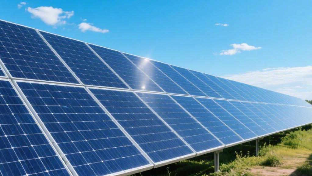
What factors affect the performance of polycrystalline photovoltaic panels?
The performance of polycrystalline silicon photovoltaic panels is primarily affected by temperature, shading, and dust accumulation.
Their standard conversion efficiency is about 15% to 17%, and when the surface temperature exceeds 25°C, the power output drops by approximately 0.4% for every 1°C increase.
Regularly cleaning surface dust with a soft brush and trimming surrounding branches to prevent the hotspot effect can effectively maintain optimal power generation.
Temperature Coefficients and Thermal Losses
Fear of Heat
When sunlight strikes the silicon wafer, photons transfer energy to electrons, causing them to jump from the valence band to the conduction band, thereby generating an electric current. As the temperature of the panel rises, the thermal vibration of atoms inside the semiconductor material intensifies, causing the bandgap to narrow.
A narrower bandgap leads to a significant drop in open-circuit voltage. Although the rising temperature causes a very slight increase in short-circuit current, the magnitude of the voltage drop far exceeds the increase in current, ultimately causing the panel's overall output power to show a clear downward trend.
In a normal temperature environment, the operational efficiency of polycrystalline silicon cells remains stable. However, once exposed to the intense heat and blazing sun of summer, the recombination rate of internal electrons significantly increases, carrier lifetime shortens, and a large amount of light energy that should have been converted into electricity is ultimately transformed into heat and dissipated into the air.
Power Loss Metrics
The maximum power temperature coefficient of polycrystalline silicon modules typically fluctuates between -0.40%/°C and -0.45%/°C. The rated power labeled on the factory nameplate is measured under Standard Test Conditions (STC), which specify an ambient temperature of 25°C, a light intensity of 1,000 W/m², and an Air Mass (AM) of 1.5.
When the actual operating temperature of the panel exceeds 25°C, the output power degrades proportionally to the aforementioned temperature coefficient for every 1°C increase. Calculating with a polycrystalline silicon panel that has a rated power of 300 W and a temperature coefficient of -0.45%/°C as an example: when the panel's own temperature reaches 65°C, it is 40°C above the standard temperature. The power degradation at this point is calculated as 40 multiplied by 0.45%, which is 18%. The panel's actual output power will decrease by 54W, maxing out at a generating capacity of only 246W.
Actual Temperature Difference
On sunny days with strong sunlight and no wind, dark blue polycrystalline silicon panels absorb a massive amount of infrared and ultraviolet heat, causing the panel's surface temperature to be 20°C to 30°C higher than the surrounding ambient air. To better approximate actual usage scenarios, the engineering sector introduced the Nominal Operating Cell Temperature (NOCT) parameter.
NOCT test conditions are set at an ambient temperature of 20°C, a light intensity of 800 W/m², and a wind speed of 1 m/s. Under these standard conditions, the actual temperature of a polycrystalline silicon panel typically reaches around 45°C to 47°C. Grasping this temperature difference data helps in estimating the true loss in power generation during the system design phase, avoiding sole reliance on ideal laboratory data for calculations. Inverter voltage matching must also account for voltage drops at high temperatures to prevent the system from triggering shutdown protection due to low input voltage during the summer.
Greenhouse Heating Effect
The installation method of the panels and the ventilation conditions of their environment drastically alter heat dissipation efficiency. Thermal convection and thermal radiation are the primary pathways for a panel to dissipate heat, with air circulation on the back being the most effective.
l During flat roof installations, the gap between the panel and the roof is usually extremely small, preventing air circulation. The heat on the back cannot be effectively carried away by the wind, causing local temperatures to climb continuously.
l When mounted on racks on the ground or flat roofs, the panels have open space in front, behind, and on both sides. Natural wind can smoothly pass through the back of the panel, utilizing air movement to carry away a large amount of waste heat, effectively lowering the operating temperature by 5°C to 10°C.
l The materials used for the panel's backsheet possess different thermal conductivities. Some polymer backsheet materials will yellow and deform under long-term high temperatures, affecting the module's overall heat dissipation performance later on.
l The aluminum alloy material of the frame has excellent thermal conductivity, assisting in conducting the heat absorbed by the glass and silicon wafers to the surrounding edges and dissipating it into the air.
Localized Heating
When one or more cells in a series circuit are shaded, the affected cells can no longer generate electricity and instead become a load, consuming the electrical energy produced by other normally functioning cells. This phenomenon rapidly drives the temperature of the shaded area up to 100°C or even higher, potentially causing the panel's backsheet to burn through, the glass to shatter, and the EVA encapsulation material to melt. To counter the heat loss caused by the sudden surge in local resistance, bypass diodes are connected in parallel within the junction box during the manufacturing process.
l When a particular string of cells experiences abnormally high impedance and heating, the bypass diode automatically turns on.
l The current bypasses the malfunctioning cell area and continues to flow through the diode.
l The bypass structure design sacrifices one-third or half of the power generation from the shaded section, but effectively prevents the entire module from catching fire or suffering permanent damage due to localized overheating.
l While in the conductive state, the diode itself generates a forward voltage drop and heat loss. The junction box design must possess good heat dissipation capabilities and is typically filled with thermally conductive silicone to control the temperature.
Heat Dissipation Rate
There are significant differences in the specific heat capacity and thermal conductivity of different materials, and their physical properties dictate the efficiency of heat transfer inside the panel. The 3.2mm ultra-clear patterned glass used on the front must not only guarantee a light transmittance of over 91% but also perform the function of rapidly radiating heat outward. The EVA film in the middle layer, acting as an insulating and bonding material, has relatively poor thermal conductivity, forming a physical barrier to outward heat conduction.
During sustained high-intensity light exposure, the thermal energy generated by the silicon wafer cannot penetrate the EVA layer instantly, creating a temporary accumulation of heat on the silicon wafer's surface. The wind speed, air humidity, and rainfall of the external environment all alter the heat exchange coefficient of the glass surface. The evaporation of moisture can carry away a massive amount of latent heat. During sunny periods following a shower, the panel temperature plummets, and the output power often experiences a massive short-term peak.
Shading, Soiling, and Hotspot Formation
Blocked Light
In conventional 60-cell or 72-cell modules, all cells are connected in series like links in a chain. When the shadow of a branch, the projection of an adjacent building, or the silhouette of a chimney falls onto the module's surface, it blocks photon input in specific areas. Inside the shaded cells, the PN junction can no longer absorb photons to excite a sufficient number of electron-hole pairs, causing a cliff-like drop in photocurrent. The entire series circuit has a mandatory requirement for current consistency; the higher current produced by unshaded, healthy cells is restricted to the lowest current threshold permitted by the shaded cells.
In a sub-string circuit containing 24 polycrystalline silicon cells, if just one cell has 20% of its light-receiving area obscured by a fallen leaf, the output current of the entire sub-string will simultaneously decrease by 20%. Because polycrystalline silicon material contains a large number of grain boundaries and defects internally, its dark current is inherently relatively high. Besides cutting off the photocurrent, localized shading also forces the cell to transition from a power source to a load within the circuit.
In a series architecture, an extremely small area of light deprivation leads to an extremely high percentage of power degradation. A tiny light-blocking obstacle can forcibly drag down the output power of the entire polycrystalline silicon panel by several times or even dozens of times due to the wooden barrel effect.
Surface Dust Accumulation
Airborne dust, industrial dust emissions, plant pollen, and bird droppings continuously settle on the protective glass of photovoltaic panels due to gravity and precipitation. These attachments alter the refractive index and reflectance of light at the air-glass interface.
The spectral response range of polycrystalline silicon cells is primarily concentrated in the visible light and near-infrared bands from 400 nanometers to 1100 nanometers. Micron-level dust particles strongly scatter light, specifically hindering the penetration of short-wave blue light, resulting in a massive reduction in the photon flux reaching the underlying EVA encapsulation film and the surface of the polycrystalline silicon wafer.
In arid deserts or regions with scarce rainfall, the dust accumulation rate is extremely high. Without effective rainfall for two consecutive months, the transmittance loss caused by the surface dust layer can reach 15% to 25%. The hazard of bird droppings is particularly prominent; their physical form is typically highly opaque and contains acidic substances. Long-term acid erosion will destroy the anti-reflective coating on the glass surface, causing the coating to peel off and leaving permanent valleys of low transmittance.
The accumulation of pollutants is not evenly distributed; the aluminum alloy frame at the bottom of the panel easily forms a water-blocking step. Muddy water brought by rainfall stagnates and dries at the frame, forming a thick band of mud that is extremely difficult to shed naturally, continuously weakening the power generation capacity of the bottom cells.
Localized Heating
When a polycrystalline silicon cell encounters severe shading or is completely covered by thick bird droppings, it faces an extreme reverse bias state. Other cells in the same series circuit that are in a normal light-receiving state will apply the voltage they generate across this shaded cell. Once the applied reverse voltage exceeds the reverse breakdown voltage threshold of the PN junction inside the polycrystalline silicon crystal, a massive current will forcefully penetrate the cell. The shaded area instantly transforms into a high-power resistive heating element.
Taking a system with a normal operating current of 9 amps as an example, if a cell experiences breakdown under a reverse voltage of 20 volts, 180 watts of electrical power will be concentrated and converted into heat inside a silicon wafer measuring just 156 millimeters square. Although the thermal conductivity of the polycrystalline silicon wafer is relatively high, the polymer encapsulation materials above and below prevent rapid heat dissipation. Localized temperatures can surge to 150 degrees Celsius or even higher within minutes.
High temperatures scorch the EVA film, causing irreversible browning and releasing corrosive gases. Sustained thermal stress will cause the polycrystalline silicon wafers to crack and the backsheet material to melt; severe localized heating is a hidden source of fire accidents in photovoltaic power stations.
Protectors
A standard 72-cell module is divided into three independent 24-cell sub-series networks, with a Schottky diode connected in parallel to each sub-network. When a cell is shaded and begins to endure reverse bias, the bypass diode connected in parallel across that sub-string will be in a forward-conducting state due to polarity reversal. The system current will bypass the obstructed 24 cells and continue transmitting through the diode.
The conduction of one diode instantly drops the operating voltage of the entire panel by one-third. A Schottky diode has a forward voltage drop of about 0.6 volts when conducting; when a large current flows through, the diode itself generates several watts of heat. If the panel is subjected to alternating tree shadows caused by moving clouds for a long time, the diode will frequently switch between conducting and blocking states. Frequent thermal cycling drastically accelerates the aging of the semiconductor PN junction. Once the diode permanently short-circuits due to thermal breakdown, one-third of the panel's power is permanently lost.
Washing Hoses
Drizzle cannot wash away surface particles; instead, it turns loose dust into a highly adhesive mud-like substance. Only a brief downpour with an intensity exceeding 5 millimeters per hour can provide an effective scouring and cleaning action on the high-transmittance tempered glass. The installation tilt angle of the panels has a polarizing effect on the retention time of dirt. Flat installations below 10 degrees easily cause rainwater to pool into puddles on the surface; after the moisture evaporates, it leaves concentric circular scale spots rich in minerals.
In dense agricultural dust areas or around heavy industrial parks, regular manual or mechanized washing is inevitable. If the concentration of calcium and magnesium ions in the cleaning water exceeds standards, it easily solidifies on the hot surface to form a hard inorganic salt crystal layer. Rough physical scraping actions will destroy the anti-reflective coating layer, which is only nanometers thick. Routine maintenance operations require precise calculation of water consumption, labor costs, and the value of the recovered electricity. Typically, maximizing economic benefits is achieved by initiating washing operations when the photoelectric conversion loss rate crosses the 4% to 5% threshold.
Irradiance and Spectral Response
Is There Enough Light
The photoelectric effect inside polycrystalline silicon semiconductor materials depends entirely on the number of electron-hole pairs excited by photons striking the surface of the PN junction.
When the external solar irradiance drops from the standard test condition of 1,000 watts per square meter to the low-light range of 200 watts per square meter, the recombination rate of minority carriers inside the polycrystalline silicon cells relatively increases. The value of the short-circuit current maintains a strict linear proportion with the incident light intensity.
As irradiance degrades exponentially, the ampere value of the photocurrent exhibits a proportional downward adjustment. The drop curve of the open-circuit voltage presents a logarithmic, non-linear characteristic.
Under extremely low light conditions, the faint voltage generated by the modules often cannot break through the minimum DC voltage threshold for the inverter to start operating. This causes the panel, despite absorbing light, to be completely in a standby, stagnant state with zero electrical output. At this time, all photoelectric conversion activities inside the system can only maintain a very weak closed loop of dark current.
Picky About Light Color
The electromagnetic radiation emitted by the sun covers a vast spectrum from high-frequency ultraviolet to low-frequency infrared. Polycrystalline silicon materials are limited by their fixed bandgap of 1.1 electron volts.
Only photons with energy higher than this value can successfully break the covalent bonds between silicon atoms, transitioning bound electrons in the valence band into the conduction band to form free charges. Photons in the infrared region with wavelengths exceeding 1,100 nanometers do not carry enough energy.
When penetrating the silicon wafer, long-wave photons only trigger lattice vibrations and convert into pure thermal energy. Although photons in the ultraviolet region with wavelengths below 400 nanometers carry massive energy, most are forcibly absorbed by the tempered glass and encapsulation film on the panel's surface.
The spectral response peak of polycrystalline silicon cells remains fixed in the near-infrared band of 800 to 900 nanometers. There is an insurmountable quantum limit loss during the conversion of photon energy into electrical energy. The excess energy difference is entirely consumed and released in the form of phonons.
Morning and Evening Differences
When the sun rises in the morning and sets in the evening, the path length of light penetrating the Earth's atmosphere far exceeds the vertical irradiation distance at noon. Air molecules cause extremely strong Rayleigh scattering of short-wavelength light.
The solar spectrum reaching the Earth's surface undergoes severe redshift. The proportion of long-wavelength red light and infrared light in the spectral structure expands drastically.
The photoelectric response sensitivity of polycrystalline silicon material in this frequency band is acceptable. However, the absolute value of the overall irradiance intensity shrinks massively, and the short-circuit current output of the panel can only be maintained at 10% to 15% of the peak period.
The constant changing of the solar elevation angle triggers a trigonometric-level reduction in the effective radiation area received by the panel surface. A mounting system with a fixed tilt angle cannot maintain the optimal light incident angle around the clock.
Cloud Thickness
Suspended particles and water vapor concentrations within the atmosphere dynamically reshape the morphology of the solar spectrum reaching the surface. Thick cumulonimbus clouds strongly obscure and scatter light.
Diffuse reflected light penetrating the bottom of the clouds takes a dominant position in the overall illumination. The proportion of high-energy short-wave blue light in the diffuse reflection spectrum is on the higher side.
The photon flux in the infrared band shrinks substantially. Because of the relatively large size of the inverted pyramid structures formed by the texturing process on the surface of polycrystalline silicon panels,
Its light-trapping capability for diffuse reflected light is somewhat sluggish. When the incident angle of light deviates from the vertical normal direction, the reflectance of the surface glass climbs rapidly, causing the total number of effective photons penetrating the surface of the internal silicon wafer to shrink further. Changes in light conditions reshape the panel's output curve at millisecond speeds.
Material Limitations
As photon-excited electrons drift towards the built-in electric field of the PN junction, they are highly prone to non-radiative recombination at such defect locations.
Against a background of high irradiance, the concentration of photogenerated carriers is massive, and some defect traps are quickly filled. Excess electrons can successfully cross the potential barrier and enter the external circuit to participate in conduction.
Once irradiance drops to a specific threshold, the capture mechanism of the defect centers over the scarce carriers gains the upper hand. The overall photoelectric conversion efficiency experiences a cliff-like drop.
The Air Mass (AM) index denotes the product of the path length of sunlight traveling through the atmosphere. Standard testing uniformly uses the AM 1.5 spectral distribution curve as a consistent reference baseline.
AM values at dawn and dusk are far greater than the standard value at noon; long-wave light is heavily absorbed and lost when penetrating the thick atmosphere. The quantum efficiency curve of polycrystalline silicon presents an extremely steep downward trend at both the infrared and ultraviolet ends, relying heavily on sustained high-intensity input in the mid-section visible light region.
Numerical Comparison
Parameter fluctuations triggered by various changes in physical conditions require detailed data references. Below is a compilation of various electrical performance values of polycrystalline silicon modules across different irradiance ranges.
Solar Irradiance (W/m²) | Short-Circuit Current Degradation Ratio | Open-Circuit Voltage Degradation Ratio | Relative Drop in Conversion Efficiency | Spectral Redshift Response Loss |
1000 | 0.0% | 0.0% | 0.0% | 0.0% |
800 | 20.0% | 1.5% | 1.2% | 0.8% |
600 | 40.0% | 3.2% | 2.8% | 1.5% |
400 | 60.0% | 5.8% | 5.1% | 2.4% |
200 | 80.0% | 12.4% | 11.5% | 4.2% |
100 | 90.0% | 22.1% | 18.7% | 7.5% |
The tabular data clearly indicates the divergent trends of current and voltage under low-light conditions. In a low photon flux environment, the complex grain boundary structures inside polycrystalline silicon materials become physical barriers hindering the smooth flow of carriers.
The low-light environment magnifies the probability of free electrons being captured by impurity recombination centers inside the material. The diffusion length of minority carriers shortens dramatically, heavily suppressing the actual fill factor value.