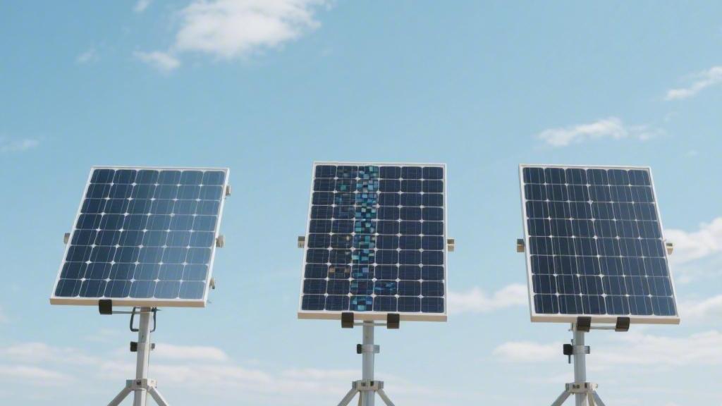
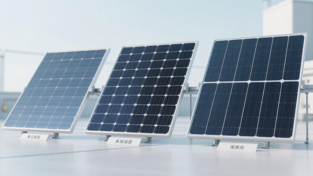
What are the 3 types of solar panels?
Monocrystalline silicon has the highest photoelectric conversion efficiency, typically above 20%. Its silicon atoms are tightly and neatly arranged, and its appearance is deep black.
Polycrystalline silicon has an efficiency of about 15% to 17% and features a blue, shattered-crystal pattern on its surface, offering a higher cost-performance ratio.
Thin-film panels utilize a flexible substrate to enable curved installations. Although their efficiency is only around 10%, they have excellent low-light response, making them suitable for complex building surfaces.
Premium & High Efficiency
How High is the Purity?
The manufacturing process of monocrystalline silicon panels begins in a quartz crucible at 1400°C. After melting high-purity polysilicon, it is slowly drawn into a cylindrical monocrystalline silicon ingot at a speed of about 1.5 millimeters per minute using the Czochralski method. The internal crystal structure has no grain boundaries, and the arrangement of silicon atoms shows a highly consistent single direction, minimizing energy loss when electrons move inside. The photoelectric conversion efficiency is generally maintained in the range of 22.5% to 24.8%. The mainstream monocrystalline silicon wafer sizes on the market are divided into three specifications: 166 mm, 182 mm, and 210 mm, with a thickness usually between 130 micrometers and 150 micrometers.
A 182 mm specification panel containing 108 half-cut cells has an overall dimension of approximately 1722 mm in length, 1134 mm in width, and 30 mm in thickness, with an overall weight fluctuating around 20.5 kg to 21.5 kg. Under standard test conditions (irradiance of 1,000 W/m², cell temperature of 25°C, air mass AM1.5), the panel can output a rated power of 400 watts to 430 watts. The open-circuit voltage is usually between 37 volts and 38 volts, and the short-circuit current is approximately 13.5 amperes to 14 amperes.
Calculated according to the current average ex-factory price in the North American market, the per-watt procurement cost of high-conversion monocrystalline silicon modules is between $0.35 and $0.50. A residential system with an installed capacity of 8 kilowatts requires about 20 panels, occupying a roof area of about 39 square meters, and the hardware cost for the panels alone is between $2,800 and $4,000.
Are They Sensitive to Heat?
In actual operation, for every 1°C increase in the physical temperature of the solar panel's surface, the output power will decrease by a specific proportion. The temperature coefficient of monocrystalline silicon panels is usually between -0.30%/°C and -0.35%/°C. At noon in summer, when the ambient temperature reaches 35°C, because the dark-colored glass absorbs a large amount of solar infrared thermal radiation, the actual physical temperature of the roof panels will soar to 65°C. Compared to the laboratory standard temperature of 25°C, the panel temperature exceeds it by 40°C. Taking a panel with a rated power of 400 watts and a temperature coefficient of -0.30%/°C as an example, the excess 40°C will result in a 12% drop in total output power.
In extreme high-temperature environments, the actual maximum output power of the panel will slide from 400 watts to 352 watts. The DC voltage received at the inverter end will also drop from 31 volts during normal operation to about 27 volts. The ventilation gap is a physical parameter that affects cooling efficiency; mounting brackets usually need to elevate the panel by 10 cm to 15 cm to ensure that the bottom air velocity reaches over 0.5 meters per second. Natural convection cooling can lower the panel's operating temperature by 5°C to 8°C, thereby recovering about 2% of the power loss.
Degradation Data
Throughout their entire life cycle of grid-connected power generation, monocrystalline silicon systems face physical losses from Light-Induced Degradation (LID) and Light and elevated Temperature Induced Degradation (LeTID). Within the first 30 to 90 days of sunlight exposure, boron-oxygen complexes inside the silicon wafer capture electrons, causing a permanent decline of 1.5% to 2.0% in the initial power generation capacity for the first year. From the second year to the twenty-fifth year, the linear degradation rate of monocrystalline silicon panels will stabilize within a narrow range of 0.25% to 0.40% annually.
l Based on a panel with a rated power of 400 watts, after 10 full years of operation, the actual output power will remain between 375 watts and 380 watts.
l By the end of the 25-year warranty period, high-end monocrystalline silicon panels can still provide 86% to 89.4% of their initial rated power.
l Assuming the panel is installed in an area with an average of 5 hours of peak sunlight per day, the theoretical power generation in the first year is 730 kWh. Considering system losses during DC to AC conversion (about 14%), the actual usable electricity is 627 kWh.
l Over the total 25-year service life, the cumulative power generation of a single panel will reach between 14,500 kWh and 15,000 kWh.
Shading Impact
In terms of physical structure, monocrystalline silicon panels are typically divided into three independent power supply zones, each monitored by a bypass diode. When the panel surface is obstructed by leaves, chimney shadows, or bird droppings, the electrical resistance of the shaded cell area will instantaneously increase, turning it from a power-generating unit into a power-consuming unit, triggering localized overheating with temperatures up to 150°C. Upon detecting a reverse bias voltage exceeding 0.6 volts, the bypass diode will immediately conduct, bypassing the current around the shaded one-third area, and the total output power of the panel will instantly drop by 33.3%.
To cope with the sudden power drop caused by shading, panels currently on the market widely adopt the half-cut cell technology. Laser cutting equipment divides standard 182 mm silicon wafers in half, so that a single panel contains 108 or 144 half-cut cells, split into upper and lower completely parallel independent circuits. When the lower half of the panel is shaded by 10% of its area due to eaves, only the bypass diodes of the lower half circuit will be activated, while the upper half of the panel can still maintain 100% full-load output.
The power loss of the entire panel is controlled at around 16.6%; compared to the 33.3% drop of traditional full-cell panels, the shade tolerance is effectively doubled. The number of internal connecting busbars has also increased from the early 5 to 9 or even 16 circular ribbons. The lateral transmission distance of current inside a single cell has been shortened by more than 40%, reducing the series resistance loss inside the panel by 1.5 watts to 2 watts.
Internal New Technologies
P-type silicon wafers are doped with boron during manufacturing, whereas N-type silicon wafers are doped with phosphorus, adding an extra free electron. N-type monocrystalline silicon completely eliminates the first-year Light-Induced Degradation (LID) caused by boron-oxygen defects, keeping the first-year degradation rate under 1%. Based on N-type wafers, TOPCon (Tunnel Oxide Passivated Contact) technology was developed, which prepares an ultra-thin silicon dioxide tunnel layer with a thickness of only 1 nm to 2 nm on the back of the cell. It allows electrons to tunnel through while blocking hole recombination, pushing the laboratory limit conversion efficiency of the cell to 28.7% and stabilizing mass production efficiency at 24.5% to 25.2%.
The back of N-type bifacial panels is also encapsulated with 2.0 mm thick tempered glass, capable of absorbing scattered light reflected from the roof or the ground. On flat-roof commercial buildings paved with white TPO roofing membranes, the surface albedo can reach 60% to 80%. The extra scattered light absorbed by the back side can provide a 5% to 15% power generation gain for the system. For a bifacial panel with a front-side rated power of 450 watts, in an environment with good albedo, the comprehensive maximum output power can break through 500 watts. Without increasing the additional installation area, the Levelized Cost of Energy (LCOE) of the overall system is reduced by 4% to 7%.
Budget-Friendly
Shattered Silicon Wafers
The manufacturing of polycrystalline silicon panels skips the time-consuming and energy-intensive Czochralski process used for monocrystalline silicon. Factories place silicon shards with a purity of around 99.999% into a quartz crucible and heat them to a melting point of 1414°C. The molten liquid silicon is poured into a square graphite casting furnace and directionally solidifies and cools at a rate of 1 to 2 cm per hour. During the cooling cycle of up to 40 to 50 hours, silicon atoms cannot form a single continuous crystal, but instead crystallize into countless independent tiny grains with physical sizes ranging from 1 mm to 10 mm. The grain boundaries formed between adjacent grains obstruct the free movement of electrons, causing photogenerated carriers to recombine when crossing the grain boundary regions, resulting in an additional electrical energy loss of about 3% to 5%.
The massive square silicon ingots are then sliced into wafers with a thickness of 160 to 180 micrometers by a diamond wire saw. Since there is no need to cut a cylinder into squares like in monocrystalline silicon production, the physical waste rate of silicon material in the polycrystalline process is significantly reduced from 25% to less than 5%. The physical size of a standard independent polycrystalline silicon wafer is usually 156.75 mm square. A conventional panel made of 60 cells connected in series has outer dimensions of approximately 1650 mm long, 992 mm wide, and 35 mm thick, with the total physical weight of a single panel typically between 18.5 kg and 19.5 kg.
Blue Tint
Because the alignment directions of the individual grains on the surface of the silicon wafer are completely different, when sunlight hits the panel surface at different angles, the incident light undergoes multi-angle diffuse reflection at the microscopic grain boundary irregularities, resulting in an uneven, frosted-glass-like texture observed by the naked eye. Factories use Plasma-Enhanced Chemical Vapor Deposition (PECVD) equipment on the silicon wafer surface to apply a silicon nitride anti-reflective coating with a thickness of 70 nm to 90 nm. The refractive index of this chemical thin film is precisely locked at around 2.05, and through the physical principle of optical interference, the surface reflectance of light waves of specific wavelengths is suppressed from an initial 30% to a minimum of 1.5%.
Short-wave blue light in the 400 nm to 500 nm wavelength range is partially reflected, giving the panel its signature deep blue appearance. The physical presence of internal grain boundaries makes it harder for infrared photons in the 800 nm to 1100 nm wavelength range to be effectively absorbed by the cells, causing the spectral response of polycrystalline panels in the long-wave band to be about 0.5 amperes to 0.8 amperes lower than that of monocrystalline panels, further dragging down the overall short-circuit current value.
Large Footprint
The average photoelectric conversion efficiency of polycrystalline silicon panels has consistently stabilized within the physical range of 15.5% to 17.5%. A 60-cell polycrystalline silicon module with a standard physical size of 1.63 square meters, under a standard test solar irradiance of 1,000 W/m², typically has a rated total output power distributed between 270 watts and 300 watts. The panel's short-circuit current is about 9.5 amperes to 10.2 amperes, and the open-circuit voltage fluctuates between 38 volts and 39.5 volts.
To build a residential roof system with a rated installed capacity of 6 kilowatts, 22 panels are required using individual 280-watt polycrystalline silicon panels. The entire array occupies a total physical roof area of 35.8 square meters. Assuming the local effective peak sun hours are 4.5 hours per day, the theoretical daily DC power generation of this system is 27.7 kWh.
After factoring in the approximately 96.5% DC-to-AC conversion efficiency of string inverters, as well as an aggregate 1.5% to 2.0% resistance heat loss from DC and AC wiring, the final usable AC electricity fed into the household distribution box is about 26 kWh. If the roof installation orientation deviates 15 degrees from true south, or the tilt angle is lower than the optimal value of the local latitude minus 15 degrees, the annual total power generation will suffer a reduction of 3% to 6.5%. In an area with an average electricity price of $0.15 per kWh, this system operating at full load for the first year can generate roughly $1,420 in electricity bill credits.
More Susceptible to Sun/Heat
The performance degradation data of polycrystalline silicon panels in high-temperature environments is more severe than that of monocrystalline panels. Its standard physical temperature coefficient is between -0.38%/°C and -0.42%/°C. At noon in summer, when the air temperature reaches 38°C, the tempered glass covered by the deep blue anti-reflective film will absorb a large amount of environmental heat, and the physical temperature of the back surface field of the panel's backsheet will soar to over 70°C. Compared to the laboratory standard test condition of 25°C, the temperature exceeds it by a full 45°C.
For a panel with a rated power of 290 watts and a temperature coefficient of -0.40%/°C, the extra 45°C will cause an absolute power degradation of 18%. The actual instantaneous output power will drop sharply from 290 watts to 237.8 watts. The voltage drop is much greater than the current drop, and the maximum power point voltage (Vmpp) of a single panel will drop from 31.5 volts under normal operating conditions to about 26.5 volts.
In an independent branch where 10 panels are connected in series, the total DC input voltage will plummet from 315 volts to 265 volts. When the start-up working voltage threshold of the inverter is 250 volts, this massive voltage drop makes it extremely easy for the inverter to fall out of the optimal voltage range for Maximum Power Point Tracking (MPPT) during the 2 to 3 hottest hours in the afternoon, causing an additional 1.5% to 2.5% loss in the system's overall daily power generation revenue.
Cheaper to Buy
The ex-factory procurement cost per watt of polycrystalline silicon modules in North America remains consistently low at $0.20 to $0.25. Compared to high-efficiency monocrystalline silicon panels priced at $0.40/watt, the procurement budget for photovoltaic hardware materials is cut by at least 37.5% to 50%.
To assemble a 6-kilowatt polycrystalline roof array, the bare hardware cost for the panels alone is between $1,200 and $1,500. However, the extremely low panel unit price will subsequently push up the costs of peripheral Balance of System (BOS) equipment. Because 280-watt polycrystalline panels have a lower power density than 400-watt monocrystalline panels, generating the same 6-kilowatt total power requires purchasing an additional 6 aluminum mounting rails each 3 meters long (unit price around $35/rail), 24 anti-corrosion stainless steel mid/end clamps (unit price around $2.5/piece), and an extra 15 meters of 10 AWG standard UV-resistant DC cables (unit price around $0.8/meter).
The matched hardware quantity of microinverters or DC power optimizers significantly increases from 15 to 22. The entire BOS auxiliary material cost will float upwards by $250 to $450 due to the increase in the absolute number of panels. After deducting the 30% federal Investment Tax Credit (ITC), a complete polycrystalline silicon roof photovoltaic system—including city building permit application fees (usually between $300 and $500) and installation labor costs (about $1.0/watt)—will have a final out-of-pocket net cost of roughly $8,500 to $10,500. The overall return on investment cycle can be compressed to 5.5 to 7.2 years.
Aging Over Time
The Light-Induced Degradation (LID) of polycrystalline silicon panels during the initial use period is usually between 2.0% and 2.5%, slightly higher than the data for monocrystalline silicon panels, and the rated power drop during the first year of grid-connected operation is the most obvious. From the second year onwards, the panel will enter a stable linear physical degradation period of 0.45% to 0.50% per year. Under long-term erosion by intense ultraviolet rays and airborne moisture, the light transmittance of the EVA encapsulant film on the back of the panel slowly decreases at a rate of 0.15% per year, resulting in a year-by-year decrease in the number of photons finally reaching the surface of the underlying cells.
The physical phenomena of thermal expansion and contraction generated by the daily cycle of day and night will, over a span of 20 years, cause tiny metal fatigue fractures in the 1.5 mm wide tin-plated copper main busbar ribbons, increasing internal series resistance by about 0.5 ohms per year. After 15 full years of continuous operation, a panel with an original factory power of 290 watts will inevitably see its actual output capacity drop to between 245 watts and 250 watts. By the end of the standard 25-year performance warranty cycle, the panel's total power generation is roughly 80% to 82% of its initial nominal value. Although the overall absolute degradation rate is about 4 percentage points higher than that of monocrystalline products, the lower initial acquisition cost keeps the Levelized Cost of Energy (LCOE) of the overall system at extremely low levels of $0.06/kWh to $0.08/kWh.
Flexible & Lightweight
Exactly How Light?
The physical thickness of thin-film solar panels is usually strictly compressed to between 1 micrometer and 2 micrometers.
Compared to traditional crystalline silicon cells with a thickness of 160 micrometers, their material volume is reduced by nearly 99.3%.
Manufacturing plants apply photovoltaic active thin films such as Cadmium Telluride (CdTe) or Copper Indium Gallium Selenide (CIGS) uniformly onto flexible polyimide plastic substrates using physical vapor deposition technology within vacuum chambers reaching temperatures of 400°C.
A standard thin-film panel with an area of 1.5 square meters has a total physical weight of only 2.5 kg to 3.2 kg.
On light steel structure roofs with a load-bearing capacity of less than 15 kg per square meter or on the roofs of aging RVs in use for over 15 years, these lightweight modules—weighing only 20% of a monocrystalline silicon panel—become the only option that meets the highest safety load-bearing coefficients.
The minimum bending curvature radius of the material can reach 0.3 meters, allowing it to perfectly adhere to the aerodynamic tops of yachts or the semi-circular surfaces of insulated tents at tilt angles greater than 15 degrees and less than 45 degrees.
In high-wind climates with wind speeds reaching 25 meters per second, the aerodynamic drag coefficient of the panel's surface is reduced by about 65% compared to traditional rigid panels installed at a 30-degree tilt.
Installers do not need to carry aluminum alloy rails that physically weigh more than 3 kg each; a single person can complete the strong industrial double-sided tape installation of a panel within 45 minutes.
This massive simplification of the installation process instantaneously drops the conventional manual installation cost of $0.80 per watt by more than 75.5%.
How Much Does it Convert?
Currently, the average photoelectric conversion efficiency of commercially mass-produced Cadmium Telluride (CdTe) thin-film panels is stably distributed within the range of 17.5% to 19.2%.
In contrast, amorphous silicon (a-Si) thin-film panels have the lowest efficiency data, maintaining only a tiny percentage range of 7% to 10%.
Although the laboratory limit conversion efficiency of Copper Indium Gallium Selenide (CIGS) materials reaches 23.4%, for mass-produced modules with an illuminated area greater than one square meter, the rated conversion efficiency drops significantly to between 13% and 15.5%.
To achieve the exact same total output power as a 6-kilowatt rated capacity monocrystalline silicon system, you would need to purchase and lay down CIGS thin-film panels covering a total area of 46 square meters.
For the same power output, the thin-film system occupies 53.3% more physical roof space than a monocrystalline silicon system with an efficiency of up to 22%.
In an area averaging 4.5 peak sun hours per day, a flexible thin-film panel with a rated power of 150 watts and physical dimensions of 1,200 mm long and 600 mm wide has a theoretical daily power generation of about 0.67 kWh.
When solar irradiance under AM1.5 air mass conditions drops from the standard 1,000 W/m² to 400 W/m² in the early morning or evening, the broad-spectrum absorption characteristics of thin-film materials make their low-light response current 12.5% to 15.4% higher than that of polycrystalline silicon panels.
In temperate oceanic climate zones with 120 rainy or cloudy days a year, this high-sensitivity low-light advantage can yield a positive data compensation of about 4% to 6.5% for the annual total power generation of the entire energy storage system.
The internal physical series resistance of the panel is typically between 2.5 ohms and 3.5 ohms, and the module's open-circuit voltage can reach 90 volts to 110 volts, while the short-circuit current is strictly limited to a low range of 1.5 amperes to 2.2 amperes.
Is It Afraid of Heat?
The operating temperature coefficient of thin-film panels consistently stays in an excellent extreme range of -0.20%/°C to -0.25%/°C.
Under extreme high-temperature conditions at summer noon, when the ambient temperature hits 38°C and the panel's physical surface temperature breaches 70°C, the 45°C temperature difference exceeding the 25°C standard test temperature will only cause the thin-film panel to lose 9% to 11.2% of its output power.
At the exact same time, a polycrystalline silicon panel with a temperature coefficient of -0.40%/°C would face a massive power drop of up to 18%.
In desert fringe areas where the number of days with peak daily temperatures exceeding 35°C reaches more than 90 days annually, the absolute daily power generation of a thin-film array in summer is 5.5% to 7.8% higher than that of a crystalline silicon array with the same rated power.
Because the back of the panel clings tightly to the roof substrate surface, completely losing the 0.5 meters/second air convection physical cooling space at the bottom, its actual operating temperature is usually 10°C to 15°C higher than that of rigid panels installed on 15 cm high aluminum brackets.
After thin-film materials are continuously baked in a high-temperature incubator at 85°C for 1,000 hours, the degradation of the Maximum Power Point (Pmax) is strictly controlled within a 5% test threshold.
During the damp-heat aging test (DH1000) at 85% relative humidity and an elevated temperature of 85°C, modules encapsulated with Polyolefin Elastomer (POE) exhibit a Water Vapor Transmission Rate (WVTR) below 0.001 g/m² per day.
This outstanding water-blocking performance compresses the probability of chemical degradation in the active layer to below 0.2%, effectively preventing leakage current from spiking from an initial 0.1 microamperes up to a highly destructive threshold of 10 microamperes.
Price Breakdown Table
Thin-film panels of different material types have a massive retail unit price fluctuation range of $0.30 to $1.50 per watt.
Thin-Film Material Type | Average Conversion Efficiency (%) | Rated Output Power (Watts) | Standard Panel Weight (kg) | Unit Price Range ($/Watt) | 10-Year Power Warranty Lower Limit (%) |
Amorphous Silicon (a-Si) | 7.5 - 9.5 | 50 - 100 | 1.5 - 2.0 | 0.85 - 1.25 | 80.5 |
Cadmium Telluride (CdTe) | 17.0 - 19.0 | 400 - 450 | 23.5 - 25.0 | 0.35 - 0.45 | 90.0 |
Copper Indium Gallium Selenide (CIGS) | 13.5 - 15.5 | 100 - 150 | 2.2 - 3.5 | 1.10 - 1.60 | 85.0 |
To build a 3-kilowatt off-grid RV system, choosing CIGS flexible thin-film panels with an average efficiency of 14% and a unit price of $1.2/watt would mean a hardware procurement budget for the panels alone as high as $3,600.
Compared to conventional monocrystalline silicon panels of the same 3-kilowatt capacity but priced at just $0.4/watt, the thin-film solution incurs an additional monetary procurement difference of $2,400.
Because the operating voltage of a single thin-film panel is as high as 90 volts or more, the system needs to be equipped with a specific model of MPPT solar charge controller capable of a maximum input voltage tolerance of 150 volts to 250 volts, with the hardware procurement cost of a single unit ranging between $250 and $450.
Although the total DC input power that the inverter needs to handle is only 3 kilowatts, matching it with 12-volt or 24-volt lithium iron phosphate deep-cycle cell banks requires ultra-thick pure copper cell connecting cables ranging from 4 AWG to 1/0 AWG, consuming an additional $80 to $150 in the accessories budget.
When 150-watt panels are connected in series into a small 450-watt string, the system operating current is physically limited to around 2 amperes, and the resistive heat loss on standard 10 AWG photovoltaic cables is less than 1.2% of the total power.
How Much Degradation?
The initial light-induced degradation (Staebler-Wronski effect) of thin-film panels occurs rapidly within the first 100 to 200 hours of the module's exposure to solar radiation.
The output power of amorphous silicon panels will experience a severe drop of 10.5% to 15.5% during the initial operating phase before the density of internal lattice defect states reaches a dynamic equilibrium value of 0.8.
The first-year overall degradation rate of Cadmium Telluride and CIGS panels is usually strictly locked between 2.0% and 3.0% by the warranty agreements signed by major manufacturers.
Starting from the second year of grid-connected operation, the annual linear physical degradation rate of thin-film materials consistently ranges between 0.50% and 0.70%.
At the 15-year milestone of continuous uninterrupted operation, a CIGS flexible panel with an initial factory nominal power of 150 watts will see its actual maximum output power drop to between 124.5 watts and 127.5 watts.
When the off-grid system reaches 25 years of service life, the remaining power generation capacity of thin-film panels roughly maintains within the range of 78.5% to 82.5% of their first-year initial rated power.
Under prolonged intense ultraviolet irradiation, the outer plastic substrate will undergo an irreversible physical phenomenon of yellowing. Overall, light transmittance decreases by about 2.5% every 5 years, leading to a cumulative 12.5% reduction in the total number of effective photons in the 300 nm to 800 nm wavelength range reaching the underlying cell surface.
After experiencing 365 cycles of massive diurnal temperature swings from 15°C to 65°C each year, the Young's modulus inside the high molecular polymer outer layer will increase by about 15.4%, causing it to gradually lose the physical flexibility that originally allowed it to bend by 30 degrees.
After 8 to 10 years of exposure to wind and sun, the moisture barrier performance of the butyl rubber sealing tape wrapped around the panel edges will drop by over 40.5%, triggering a 0.5% to 1.5% localized oxidation reaction in the internal indium and gallium metals.
Long-term seal aging leads to the probability of the bypass diode being activated by high impedance spiking from an initial 0.1% to 3.5% by the 15th year for a single panel, increasing the annual average fault repair frequency of the entire system by 0.2 times.