Which of the 3 Main Types of Solar Panels are the Most Efficient
Among the three major types of solar panels, monocrystalline panels have the highest efficiency, with a photoelectric conversion rate typically reaching 20%-24%.
They are made from high-purity single silicon crystals. In practical applications, if your installation space is limited, it is recommended to directly purchase monocrystalline panels to maximize power generation per unit area.
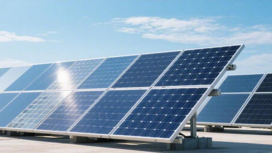
Monocrystalline Panels
The purification temperature for manufacturing monocrystalline silicon panels needs to be continuously maintained in a high-temperature range of 1400°C to 1500°C to melt the raw silicon and pull it into a cylindrical silicon ingot with a single crystal orientation. The physical purity of the silicon pillar produced by the purification process reaches 99.999%, and the probability of atomic arrangement error inside the crystal is suppressed below 0.001%.
The factory uses a 60-micrometer diameter diamond wire to cut a 210-millimeter diameter silicon ingot into thin wafers with a thickness between 130 micrometers and 150 micrometers. The cutting rate of a single machine is about 3000 pieces per hour. After phosphorus diffusion treatment at a temperature of 850°C to 900°C, a PN junction with a thickness of about 0.3 micrometers to 0.5 micrometers is formed on the surface of the silicon wafer, generating an open-circuit voltage of 1.5 volts to 2 volts.
l Furnace temperature parameters: 1400°C to 1500°C.
l Silicon raw material purity indicator: 99.999%.
l Wafer thickness specifications: 130 micrometers to 150 micrometers.
l PN junction thickness dimensions: 0.3 micrometers to 0.5 micrometers.
Currently, the photoelectric conversion efficiency of mass-produced N-type monocrystalline silicon panels stabilizes in the maximum value range of 22% to 24.5%, an increase of about 4 percentage points compared to the industry median baseline five years ago. A standard panel consisting of 108 half-cut cells has dimensions of 1722 mm long and 1,134 mm wide, with an overall light-receiving surface area of approximately 1.95 square meters.
Under a standard test illumination density of 1000 watts/square meter, the nominal output power of a single panel can reach 400 watts to 430 watts, and the production capacity per square meter exceeds 210 watts. After adopting the 72-cell format with dimensions expanded to 2278 mm by 1,134 mm, the full-load output power of a single module jumps to 570 watts to 610 watts, and the operating current increases to 13 amperes to 14 amperes. Half-cut technology splits the conventional 10-ampere current in two, reducing it to about 5 amperes, which drastically reduces the internal resistance power loss ratio by 75%.
l Photoelectric conversion efficiency: 22% to 24.5%.
l 108-format dimensions: 1722 mm x 1,134 mm.
l Power per unit area: >210 watts/square meter.
l Resistance loss reduction rate: 75%.
The surface of a monocrystalline silicon cell is printed with 9 to 16 main busbars, and the deposition width of the silver paste is only 0.1 mm to 0.15 mm. The high-density busbar arrangement shortens the physical distance that current conducts on the wafer surface by 2 mm to 3 mm, reducing the internal series resistance value by approximately 15%.
The thickness of the anti-reflective coating covering the glass surface layer is precisely controlled at 70 nanometers to 90 nanometers, which can reduce the visible light reflectance in the 380-nanometer to 1100-nanometer wavelength range from 4% to below 1%. Coated glass with a light transmittance exceeding 94% adds an effective photon capture rate of approximately 2% to 3% for a single panel.
l Number of main busbars: 9 to 16.
l Silver paste width specifications: 0.1 mm to 0.15 mm.
l Anti-reflective coating thickness: 70 nanometers to 90 nanometers.
l Glass light transmittance: >94%.
The standard test temperature baseline for monocrystalline panels is set at 25°C, but the actual operating environment temperature on summer roofs usually climbs to the 45°C to 65°C range. Its power temperature coefficient median currently sits between -0.26%/°C and -0.30%/°C; for every 1°C increase in temperature, the actual electricity generated decreases by 0.26% to 0.30%.
When the physical temperature of the panel's backsheet surface reaches a peak of 65°C, the negative deviation of the total power will reach -10.4% to -12%. Under a normal Nominal Operating Cell Temperature (NOCT) of 45°C, the actual steady-state power output of a nominally 400-watt panel fluctuates between 300 watts and 315 watts, experiencing a conversion rate degradation of about 20% to 25%.
l Standard test temperature: 25°C.
l Power temperature coefficient: -0.26%/°C to -0.30%/°C.
l 65°C high-temperature power loss: -10.4% to -12%.
l NOCT calibrated output ratio: 75% to 78.75%.
Three bypass diodes are installed inside the rear junction box of a monocrystalline silicon panel, responsible for monitoring the operating voltage fluctuations of three independent series circuits at a frequency of 0.1 seconds. When the panel surface is obscured by leaves or bird droppings covering about 33% of the light-transmitting area, the local hot spot temperature will instantly rise to 80°C to 100°C within 3 minutes.
The diodes sense a reverse voltage deviation value exceeding 0.5 volts and immediately block the 10-ampere to 13-ampere current loop of the shaded area. The physical blocking mechanism rigidly reduces the overall power loss caused by shadow coverage from 100% to 33.3%, controlling the probability of local modules burning out due to overheating within a standard error of 0.005%. When used with micro-inverters, a 15% efficiency drop in a single panel will never affect the 7200-watt total load capacity of the other 10 to 15 normal panels in the same circuit.
l Number of diodes: 3.
l Monitoring response speed: 0.1 seconds.
l Hot spot extreme temperature: 80°C to 100°C.
l Shadow power guaranteed ratio: 66.7%.
The factory-configured linear power warranty period for monocrystalline silicon products spans a length of 25 to 30 years. During the first 12-month cycle after installation, the initial Light-Induced Degradation (LID) rate of the panel is strictly limited to a percentage range of 1% to 2%. Moving from the 2nd year to the 30th year of use, the annual average power decline probability remains at 0.4% to 0.5%, and the remaining output power at the 25-year lifespan cutoff point remains above 87.4% to 89% of the initial nominal value.
The 3.2-millimeter thick tempered glass on the front of the panel can withstand a static snow pressure load of 5400 Pascals, and the anodized aluminum alloy frame structure on the back resists a wind pressure intensity of 2400 Pascals. Distribution data from impact tests show that when struck by hail with a diameter of 25 mm falling at a speed of 23 meters/second, the probability of micro-cracks on the glass surface layer is less than 0.1%.
l Warranty period span: 25 to 30 years.
l First-year LID rate: 1% to 2%.
l Annual power degradation rate: 0.4% to 0.5%.
l Front snow load strength: 5400 Pascals.
The ex-factory bare board shipping price for manufacturing N-type monocrystalline silicon modules currently fluctuates in the low range of $0.25 to $0.30 per watt. The total terminal bill, including the AC inverter system, roof mounting hardware, and installation labor costs, is fixed at $2.5 to $3.0 per watt when calculated based on a 10-kilowatt system full-load capacity.
A 10-kilowatt monocrystalline power generation facility with an initial total budget expenditure of $25,000 to $30,000 can produce approximately 15,000 kilowatt-hours (kWh) of electricity over 365 days in geographical latitude areas with an annual average of 1500 hours of sunshine. Calculated at a median utility grid rate of $0.15 per kWh, this system can provide a monetized return of $2,250 every 12 months.
Taking into account the 0.5% annual power generation reduction variance, the capital payback period to 100% cover the initial budget falls within a timeline of 6.5 to 7.5 years. Amortized over a 25-year physical lifespan, the Levelized Cost of Energy (LCOE) drops to a data range of $0.04 to $0.06 per kWh, which is about 60% to 70% lower than traditional grid rates.
l Ex-factory per-watt cost: $0.25 to $0.30.
l Terminal installed unit price: $2.5 to $3.0.
l LCOE per kWh cost: $0.04 to $0.06.
l Investment payback period: 6.5 to 7.5 years.
Polycrystalline Panels
The purification furnace temperature for manufacturing polycrystalline silicon panels is maintained in the range of 1300°C to 1400°C. The factory places silicon fragments into a quartz crucible to melt, and then solidifies them into square silicon ingots containing multiple crystal orientations within a controlled physical cooling cycle. Fluctuations in the cooling rate cause the median purity of the final silicon block to remain at 99.99%, and the probability of internal impurities is about 0.005% higher than that of monocrystalline silicon.
The assembly line uses steel wires with a diameter of 80 micrometers to 100 micrometers to cut square silicon ingots weighing up to 800 kilograms into wafer slices with a thickness between 150 micrometers and 180 micrometers. Because the complex process of pulling a single crystal pillar is not required, the overall energy consumption of manufacturing 1 megawatt of polycrystalline silicon cells is reduced by about 20% compared to monocrystalline silicon. The standard wafers cut out present perfect square edges, usually 156.75 mm in length by 156.75 mm in width, achieving a maximum area utilization rate of 100%.
The purification temperature parameters are set at 1300°C to 1400°C, the silicon wafer thickness specifications are kept at 150 micrometers to 180 micrometers, the physical dimensions of a single piece are fixed as an absolute square of 156.75 mm, and the overall production energy consumption reduction rate reaches 20%.
For polycrystalline silicon panels currently circulating in the market, the distribution sample of their photoelectric conversion efficiency is mainly concentrated in the 15% to 18% range. A conventional panel assembled from 60 standard cells has physical dimensions of approximately 1650 mm long and 992 mm wide, occupying a physical area of 1.63 square meters. Under an illumination radiation intensity of 1000 watts per square meter, the peak output power of a single panel falls within a statistical range of 270 watts to 300 watts, and the production capacity density per unit area is approximately 165 watts to 184 watts per square meter.
On cloudy days or in the morning and evening when the light incidence angle is below 30 degrees, the multi-directional crystalline structure on the surface of polycrystalline silicon can capture additional scattered light, allowing the power output ratio in low-light environments to show a slight positive deviation of 0.5% to 1%. When the load is connected to an AC system with a rated power of 5000 watts, the operating voltage of the polycrystalline silicon array is usually maintained in the 30-volt to 35-volt range, with a median output current of 8 amperes to 9 amperes.
The median photoelectric conversion efficiency falls between 15% and 18%, the area of a 60-cell panel is 1.63 square meters, the maximum output power range of a single panel is 270 watts to 300 watts, and the power generation increase rate in low-light environments is 0.5% to 1%.
Observing the physical appearance of polycrystalline silicon cells, the surface presents a fragmented distribution of dark blue to light blue ice-pattern textures formed by reflections from different crystal grains. To minimize the probability of photon loss, the thickness of the silicon nitride anti-reflective coating covering the wafer surface is controlled between 75 nanometers and 80 nanometers.
Due to the large variance in surface flatness of the polycrystalline structure, the coating still produces a surface light reflectance of 2% to 3% for the solar spectrum with wavelengths from 400 nanometers to 1100 nanometers. The front of the cell is printed with 5 to 9 main busbars, which are subjected to high-temperature sintering using conductive silver paste with a width of 0.15 mm to 0.2 mm, responsible for pooling internal electrons into an outputtable DC current. The physical distance between adjacent busbars has increased by about 1.5 mm, resulting in an internal electron transmission resistance loss rate that is about 3% to 5% higher than that of monocrystalline silicon.
The anti-reflective coating thickness is controlled at 75 nanometers to 80 nanometers, the surface beam reflectance is maintained at 2% to 3%, the distribution of the number of main busbars is 5 to 9, and the width of the conductive silver paste is 0.15 mm to 0.2 mm.
During the summer high-temperature operational cycle, the power temperature coefficient of polycrystalline silicon panels is usually fixed in a data range of -0.35%/°C to -0.40%/°C. Using a standard laboratory test temperature of 25°C as the baseline, for every 1°C climb in ambient air temperature, the actual output power generated by the system will experience a negative degradation of 0.35% to 0.40%.
When roof environments cause the absolute temperature of the panel's backsheet to reach a maximum peak of 65°C, a single nominally 280-watt panel will endure a power loss of 14% to 16%, and the actual working value will drop to a range of 235 watts to 240 watts. In statistical samples where the Nominal Operating Cell Temperature (NOCT) reaches 45°C, the voltage dispersion of the polycrystalline silicon module will expand, and the overall photoelectric conversion efficiency faces a rigid reduction of 22% to 26%.
The power temperature coefficient falls between -0.35%/°C and -0.40%/°C, the power reduction rate brought by a 65°C high-temperature environment reaches 14% to 16%, and the conversion rate reduction magnitude at a 45°C nominal operating temperature is 22% to 26%.
Polycrystalline silicon modules packaged by legitimate factories come with an expected physical lifespan and linear power warranty period that is equally as long as 25 years. In the first 12 months after connecting to the grid for operation, the impurity complex reactions inside the crystal will bring about an initial Light-Induced Degradation (LID) rate of 2% to 2.5%. Advancing along the timeline from the 2nd year to the 25th year, the annual average power reduction rate of the panel is calibrated in the range of 0.5% to 0.6%.
Upon reaching the end of the 25-year lifespan cycle, the probability of the system's remaining minimum effective output power can still be maintained above 80% to 82.5% of the ex-factory nominal value. The 3.2-millimeter low-iron ultra-clear patterned glass, paired with an aluminum alloy frame approximately 1.5 millimeters thick, can withstand a static snow load gravity of 5400 Pascals and a dynamic wind pressure intensity of 2400 Pascals in mechanical strength tests.
The first-year initial light-induced degradation rate is 2% to 2.5%, the annual average power reduction rate remains at 0.5% to 0.6%, the remaining power ratio at the end of the 25-year usage cycle is greater than 80%, and it endures a static snow load strength of 5400 Pascals.
In the current supply chain system, the median ex-factory price for bare polycrystalline silicon boards is suppressed to a range of $0.18 to $0.22 per watt. The final terminal installation price, including inverters, wiring materials, and labor costs, puts the unit price for a 10-kilowatt capacity system at approximately $2.00 to $2.30 per watt. The initial construction total budget cost falls between $20,000 and $23,000, but under the same 10-kilowatt installed capacity, polycrystalline silicon panels require an additional 15% to 20% of roof area, expanding the total area requirement to 60 to 65 square meters.
In geographical locations with an annual average effective sunshine duration of 1500 hours, the total power generation of this system in one year is about 14,000 kWh. Calculated at a utility price of $0.15 per kWh, the annual total monetary return is $2,100. Factoring in an annual 0.6% power generation reduction variance, the investment return payback period to fully recoup the $20,000 initial budget will be extended to a span of 7.5 to 8.5 years. Amortizing all hardware costs and maintenance costs over the 25-year lifecycle, its Levelized Cost of Energy (LCOE) statistical value falls between $0.05 and $0.07 per kWh.
The median ex-factory per-watt price is $0.18 to $0.22, the terminal system unit price range is $2.00 to $2.30, the initial construction budget for a 10-kilowatt capacity is $20,000 to $23,000, and the investment return payback period span is 7.5 to 8.5 years.
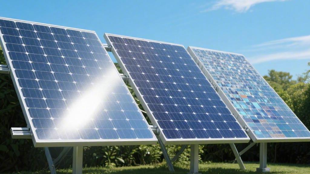
Thin-Film Panels
Manufacturing thin-film solar panels does not require going through 1400°C high temperatures to melt silicon raw materials. Factories convert photovoltaic materials into a gaseous state, and within a vacuum deposition chamber maintained at 400°C to 500°C, attach the gaseous atoms layer by layer to the substrate surface. Without the prerequisite of pulling high-purity silicon crystals, the electrical energy consumption value of the entire manufacturing assembly line is reduced by approximately 30% to 40% compared to crystalline silicon panels.
The thickness of the deposited active photovoltaic coating is typically only 1 micrometer to 2 micrometers, occupying merely 0.6% to 1.3% of the 150-micrometer physical thickness of a conventional monocrystalline silicon wafer. This extremely low thickness indicator allows equipment to carry out continuous spraying operations on 3 different types of substrate materials: glass, stainless steel foil, or polyimide plastic film.
The production equipment uses a roll-to-roll continuous operating speed; a single machine can advance the substrate material forward by 2 meters to 3 meters per minute, and the variance in atomic distribution within the coating material is forcibly kept below an error rate of 0.005% by sensors. Three basic types of compounds, including Cadmium Telluride (CdTe), Copper Indium Gallium Selenide (CIGS), and Amorphous Silicon (a-Si), form microscopic electronic layers with semiconductor characteristics within controlled curing cycles.
Production Stage Parameters | Quantified Value Samples |
Vacuum deposition chamber temperature | 400°C - 500°C |
Production process energy consumption reduction rate | 30% - 40% |
Active photovoltaic coating thickness | 1 micrometer - 2 micrometers |
Roll-to-roll coating advancement speed | 2 meters/min - 3 meters/min |
Coating atomic distribution variance | < 0.005% |
For thin-film modules mass-produced and circulating in the market, the sample range of their photoelectric conversion efficiency overwhelmingly falls into a low-level probability distribution of 10% to 13%. Under a standard irradiance test of 1000 watts per square meter, a 1-square-meter area of thin-film material can only produce a stable output power of 100 watts to 130 watts. When a user needs to meet the installed capacity of a 10-kilowatt AC load system, the site must provide approximately 80 to 100 square meters of available installation space, occupying about 100% more physical surface area than a monocrystalline silicon array.
On rainy days, when the illumination radiation intensity drops to 100 watts to 200 watts per square meter, thin-film materials can absorb the ultraviolet band of the spectrum with wavelengths falling in the 300-nanometer to 400-nanometer range. Every morning during the weak illumination period when the solar incidence angle is between 10 degrees and 20 degrees, the array can reach the 50-volt minimum activation voltage to start the inverter 1.5 hours earlier than conventional panels. Placed in a temperate climate where humidity is greater than 70% and sunshine frequency is severely broken up by cloud cover, this system's total power output over 365 days will generate a positive deviation gain of about 5% to 7.5%.
Power Generation Efficiency Data | Quantified Value Samples |
Median photoelectric conversion efficiency | 10% - 13% |
Standard output power per square meter | 100 watts - 130 watts |
10-kilowatt system area requirement | 80 sq meters - 100 sq meters |
Inverter early activation time | 1.5 hours |
High humidity environment power increase rate | 5% - 7.5% |
After stripping away the conventional aluminum alloy hard peripheral frame, the overall thickness of a thin-film panel based on a polymer plastic substrate is drastically compressed to between 2 millimeters and 4 millimeters. The physical design devoid of any rigid support plummets the static mass per square meter straight down to an extremely low baseline of 2.5 kilograms to 3.5 kilograms. Geared towards lightweight corrugated steel roofs where the load-bearing limit is strictly restricted to under 10 kilograms per square meter, the extremely low deadweight parameter completely exempts the initial construction budget cost of adding extra load-bearing steel beams.
Observing the surface details from the exterior, the entire panel presents an absolutely uniform solid dark black or dark brown visual texture, and the silver conductive busbar structures used for convergence on the front of the wafer are completely hidden. Thanks to the physical flexibility parameters of the active materials themselves, models based on stainless steel film or plastic substrates can withstand a physical arc bend with a radius of 0.5 meters to 0.8 meters. When subjected to surface amplitude fluctuations generated by wind speeds of 20 meters per second, the probability of invisible micro-cracks occurring inside the coating is about 85% lower than that of brittle crystalline silicon materials.
Physical Specification Parameters | Quantified Value Samples |
Polymer substrate panel thickness | 2 mm - 4 mm |
Frameless panel weight per square meter | 2.5 kg - 3.5 kg |
Tolerable physical bending radius | 0.5 m - 0.8 m |
Micro-crack occurrence probability reduction rate | 85% |
Surface visible light reflectance | < 1.5% |
During extreme summer cycles when actual absolute temperatures climb in the roof environment, thin-film materials exhibit an excellent power temperature coefficient among current photovoltaic products, with test data calibrated in the numerical range of -0.20%/°C to -0.25%/°C. The laboratory continuously adds temperature variables to the standard 25°C air temperature; for every 1°C increase on the scale, the output power of the thin-film panel only undergoes a negative downward slide of 0.20% to 0.25%.
When intense infrared radiation at noon heats the physical temperature of the panel's back to a maximum peak of 65°C, the power loss of the panel's total rated power is still suppressed within an 8% to 10% range. In test parameters where the Nominal Operating Cell Temperature (NOCT) is calibrated at 43°C, a thin-film array with a nominally rated full-load power of 300 watts can still maintain an actual steady-state output lumen at a relatively high proportion of 270 watts to 276 watts. The flat structure, which is only a few millimeters thick, has no internal air layer, and its discharge rate of physical heat dissipating into the external environment is about 1.5 times faster than modules with thick glass backsheets.
Thermodynamic Reaction Data | Quantified Value Samples |
Power temperature coefficient | -0.20%/°C - -0.25%/°C |
65°C environment power slide magnitude | 8% - 10% |
Nominal Operating Cell Temp (NOCT) | 43°C |
NOCT state actual output ratio | 90% - 92% |
Physical heat dissipation rate increase | 1.5 times |
The linear power warranty period for conventional thin-film products on the market is set within a time span of 10 to 15 years, and the coverage time for a small number of CIGS models is extended to 20 years. During the first 12 months of stable operation incorporated into the AC grid, the initial Light-Induced Degradation (LID) rate of the coating material typically produces an initial loss value of 3% to 4%. Advancing to the time distribution band from the 2nd year through the 15th year, the annual average power drop variance is set at a fixed frequency of 0.7% to 0.8%.
When reaching the end time node of the 15-year usage cycle, the median lowest effective power generation maintained by the entire system roughly stays between 75% and 80% of the ex-factory full-load nominal value. The physical smearing width of the edge sealing tape of the product is strictly limited to a standard of 10 mm to 15 mm, because chemical coating materials extremely easily absorb water molecules in the ambient air. If physical damage resulting in edge seal peeling occurs in regions where humidity parameters are greater than 85% year-round, the photoelectric conversion degradation rate of the coating will increase by 1.2 times to 1.5 times within a 3-month period.
Lifespan and Degradation Parameters | Quantified Value Samples |
Linear power warranty time span | 10 years - 15 years |
First-year LID rate | 3% - 4% |
Annual average power drop rate | 0.7% - 0.8% |
15-year endpoint remaining power median | 75% - 80% |
Edge sealing tape physical width | 10 mm - 15 mm |
On current global supply chain assembly lines, the per-watt billing price for bare thin-film boards is currently at an absolute low numerical level of $0.20 to $0.25. Factoring in the AC inverter hardware, DC cables, and installation team labor billing amounts required for a 10-kilowatt system, the final terminal delivered unit price handed over to the user is controlled at roughly $2.00 to $2.50 per watt. Due to the extremely low mass parameter of the panel itself, construction teams can correspondingly reduce the procurement quantity of metal brackets, deducting a deviation amount of $0.10 to $0.15 downward from the per-watt physical construction cost.
Allocating a monetary budget of $20,000 to $25,000 to deploy a 10-kilowatt capacity array, placed at latitude and longitude coordinates where the annual average continuous sunshine duration reaches 1500 hours. Because the maximum photoelectric conversion rate is limited by physical attributes, the total power throughput of the system over 365 days a year hovers around the numerical range of 12,000 kWh.
Converting this using a local utility rate of $0.15 per kWh, the entire system can generate an annual revenue figure of approximately $1,800. Factoring the 0.8% annual diminishing degradation rate into the calculation model, the financial payback period to fully recoup the $20,000 initial budget falls within a time span of 11 to 13 years. Calculating the Levelized Cost of Energy (LCOE) for a 15-year life cycle, the unit price figure is fixed in the distribution range of $0.06 to $0.08 per kWh.