Can a Solar Cell Work without a PN Junction | 3 Alternatives
The answer is yes.
Traditional PN junctions are not the only choice; charge separation can be achieved through the following three alternative solutions:
1. Schottky Junction, which utilizes the contact between metal and semiconductor to form a barrier, simplifying the manufacturing process;
2. Bulk Heterojunction (BHJ), formed by blending donor and acceptor materials, with efficiency in organic solar cells already exceeding 19%;
3. Ferroelectric Effect, relying on the spontaneous polarization within the crystal to generate current, where the open-circuit voltage can far exceed the bandgap of the material.
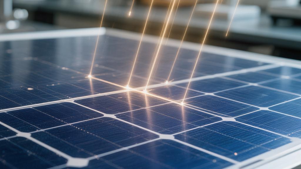
The Schottky Junction
How it Generates Power
Schottky junctions work by utilizing the electric field generated at the contact surface between a metal and a semiconductor, without needing to create a boundary between P-type and N-type within the silicon wafer like traditional batteries.
When a gold atom layer with a work function of 5.1 electron volts (eV) comes into contact with N-type silicon with a work function of 4.05 electron volts (eV), a potential difference of approximately 1.05 volts (V) is generated at the interface.
This physical contact forms a space charge region within a depth of 0.1 microns to 0.5 microns, producing a built-in voltage of about 0.65 volts (V), which is sufficient to pull apart the electrons and holes generated by light.
Under standard AM1.5 lighting conditions, the speed of charge separation at this interface can reach 100,000 meters per second, which is about 15% faster than the charge drift speed in ordinary batteries.
Since it does not require high-temperature treatment above 1000°C like PN junctions, the carrier lifetime of the silicon wafer can be maintained at over 500 microseconds, reducing energy quenching by about 10%.
Material Selection
When choosing contact metals, noble metal thin films with a thickness between 8 nanometers and 15 nanometers, such as gold, platinum, or palladium, are typically used.
If the metal layer thickness exceeds 20 nanometers, more than 45% of visible light will be reflected or absorbed, resulting in a reduction of over 30% in the number of photons entering the silicon substrate.
Using a gold thin film with a conductivity of 4.52×10⁷ S/m ensures a short-circuit current of about 38 milliamperes (mA) on an area of 1 square centimeter.
If an attempt is made to thin the metal layer to 5 nanometers to increase light transmittance to over 90%, the sheet resistance of the film will jump from 20 ohms per square to 80 ohms, causing the total conversion efficiency of the cell to drop by about 2.5 percentage points.
Current mainstream research tends to add a 0.5 nanometer thick lithium fluoride (LiF) layer as a modification layer at the interface, which can increase the Schottky barrier height by about 0.15 electron volts (eV), thereby increasing the open-circuit voltage by about 12%.
Effortless Manufacturing
Production of this cell avoids the 120-minute high-temperature diffusion process, opting instead for magnetron sputtering or electron beam evaporation in a vacuum environment of 10⁻⁵ Pa.
The entire deposition process can be completed within 300 seconds, and the ambient temperature is always maintained between 25°C and 100°C, reducing electricity consumption by 92% compared to traditional processes.
On a 100-piece scale experimental line, the processing cycle for a single piece has been significantly compressed from 180 minutes to less than 20 minutes.
This room-temperature process means that flexible plastic substrates with a thickness of only 50 microns can be used, without bearing the 15% scrap rate risk of traditional silicon wafers being easily warped and damaged at high temperatures.
In terms of equipment investment, the hardware budget for building a Schottky cell workshop with an annual output of 50 megawatts (MW) is only about 12 million yuan, saving about 65% in initial investment compared to traditional production lines.
Efficiency Performance
Currently, the conversion efficiency of silicon-based Schottky batteries prepared in laboratories generally fluctuates between 14.5% and 17.8%.
The main efficiency loss comes from about 10% specular reflection on the metal surface and an interface state density as high as 10¹² cm⁻²eV⁻¹.
These defects cause about 18% of photogenerated electrons to recombine before flowing out of the cell.
To compensate for this drawback, researchers have introduced a 2 nanometer thick graphene oxide layer between the metal and silicon, which has improved charge collection efficiency by about 11.5%.
In a 240-hour continuous light test, the efficiency decay rate of unencapsulated batteries was about 4.2%, while modules encapsulated with fluoropolymer maintained an efficiency rate of over 96.5% after working for 1,000 hours at a high temperature of 50°C.
Compared to the efficiency of traditional monocrystalline silicon batteries, which is over 24%, the Schottky solution is about 6 percentage points lower, but it has a comparative advantage of 20% in power output per unit cost.
Cost Savings
From the perspective of cost structure, the manufacturing cost of modules per watt of power generation capacity can be reduced from 0.16 US dollars to about 0.07 US dollars, a decrease of 56%.
As the manufacturing steps are simplified from the traditional 14 steps to 6 steps, the material flow speed in the factory has increased by 1.2 times.
In areas with an annual sunshine duration of 1500 hours, the static payback period for this low-cost solution is about 4.5 years, which is about 38% shorter than that of traditional distributed photovoltaic systems.
Considering a 15% equipment depreciation rate after 5 years, the internal rate of return (IRR) is expected to remain at a high level of about 19%.
In terms of raw material consumption, each square meter of cell requires only about 0.2 grams of gold or equivalent noble metals.
Through a recycling system, more than 98% of the metal can be recycled, making the residual value after decommissioning about 300 yuan per kilowatt higher than that of ordinary modules.
Dye-Sensitized Solar Cells
Generating Power Like Leaves
When photons with an energy of 1.8 electron volts (eV) hit dye molecules (such as the commonly used N719 ruthenium-based dye), electrons jump from the ground state to the excited state and are then instantly injected into the conduction band of titanium dioxide.
Due to the diameter of titanium dioxide particles being only 20 nanometers, this tiny size creates a massive surface area.
The effective surface area per gram of this white powder is as high as 100 square meters, equivalent to half the size of a tennis court, which allows it to adsorb more than 1000 times more dye molecules than a flat surface.
Under standard lighting, this structure can generate a current of about 18 to 22 milliamperes (mA) per square centimeter.
The diffusion length of electrons traveling through the titanium dioxide particle network can reach 20 microns, which is enough to collect them onto the conductive glass base before charge loss occurs.
· Injection Speed: 100 femtoseconds (0.1 picoseconds)
· Voltage Output: Open-circuit voltage is usually between 0.7 volts and 0.85 volts
· Surface Area Ratio: Specific surface area can reach over 100 square meters per gram
· Layer Thickness: The thickness of the light-absorbing layer is distributed between 8 and 15 microns
Details of White Powder
To ensure good conductivity, the printed film needs to be heated in an air furnace at 450°C for 45 minutes to form firm sintered necks between the 20 nanometer particles.
This sintering process forms a porosity of about 50% to 60%, facilitating the penetration of liquid electrolyte into every corner.
Experimental data shows that if the particle size increases to 100 nanometers, although the light transmittance will improve, the total surface area will shrink by more than 80%, causing the cell efficiency to drop from 10% to below 3%.
To further enhance light-trapping capabilities, researchers often add a layer of 400 nanometer large particles as a reflection layer at the bottom, which can increase the utilization rate of long-wavelength photons by about 15%, adding an extra 2 milliamperes per square centimeter to the short-circuit current density.
Dye Capturing Photons
Dye molecules are responsible for capturing visible light between 400 nanometers and 800 nanometers in the solar spectrum.
The most stable N719 dye has a high extinction coefficient of 14,000 liters per centimeter per mole at the 530 nanometer wavelength, which means only an extremely thin layer is needed to absorb more than 90% of incident light.
In addition to expensive ruthenium-based metal dyes, the cost of fully synthetic organic dyes is only about 10% of theirs, and a conversion efficiency of 13% has been achieved in the laboratory.
These molecules are anchored to the titanium dioxide surface through carboxyl groups (-COOH), and the binding force is strong enough to withstand wind pressure vibrations at speeds of 120 kilometers per hour.
In a standard 10 cm by 10 cm module, the amount of dye used is only a few milligrams, but it determines the total power generation over the 20-year lifespan of the entire panel.
· Absorption Range: 400 nanometers to 850 nanometers band
· Adsorption Density: Approximately 10 to the power of -7 moles per square centimeter
· Extinction Coefficient: Between 14,000 and 25,000 (unit L/mol cm)
· Molecular Size: Approximately 1 nanometer to 2 nanometers
Liquid Transferring Charge
Dye molecules that have lost electrons are in an oxidized state and must rely on the iodide (I-/I3-) redox pair in the liquid electrolyte to be reduced.
The concentration of this liquid "potion" is usually maintained at 0.5 moles per liter, and it fills the entire titanium dioxide pores through capillary action.
After electrons travel through the external circuit and return, they react with the electrolyte on the counter electrode coated with an extremely thin platinum layer (about 5 nanometers thick) to complete the charge loop.
Although liquid electrolytes pose risks of leakage or volatilization at high temperatures above 80°C, the working temperature range can be widened to between -40°C and +85°C by using ionic liquids or solid polymer electrolytes.
Currently, advanced encapsulation technology can ensure that the solvent loss of liquid modules after 1000 hours of outdoor exposure is less than 1% of the total mass.
Ferroelectric Solar Cells
Relying on Spontaneous Force
Inside ferroelectric materials, the centers of positive and negative charges are inherently offset in the lattice structure, which forms a constant, full-coverage electric field throughout the crystal, with strengths typically between 100,000 volts and 1,000,000 volts per centimeter.
When the photon energy exceeds the material's bandgap (usually between 2.2 and 3.5 electron volts), the excited electrons and holes are immediately pulled by this global electric field and drift rapidly in opposite directions.
Since the electric field is distributed in every atomic space of the material, the charge separation path is shortened from several microns in traditional PN junctions to the nanometer level, which greatly increases the collection probability of charges before they are recombined.
In a thin film sample with a thickness of 100 nanometers, this polarization intensity can reach 60 to 100 microcoulombs per square centimeter.
Performance Index | Traditional Monocrystalline Silicon (PN Junction) | Ferroelectric Thin Film (BFO Material) |
Open-Circuit Voltage | 0.6 to 0.75 Volts | 3 to over 50 Volts |
Working Mechanism | Interface electric field separation | Bulk effect global separation |
Thickness Specification | 160 to 180 Microns | 50 to 500 Nanometers |
Photo-response Speed | Microsecond level | Nanosecond level |
Carrier Collection Distance | 10 to 100 Microns | 10 to 100 Nanometers |
Theoretical Efficiency Limit | 29.4% (SQ Limit) | Theoretically can break the SQ Limit |
Voltage Can Go Off the Charts
In traditional photovoltaic theory, the cell voltage can never exceed the bandgap width of the semiconductor.
However, under the ferroelectric architecture, due to the existence of countless nanometer-scale ferroelectric domains, each domain boundary acts like a miniature cell.
Thousands of miniature batteries are stacked in series, ultimately outputting a startlingly high voltage at the two macroscopic electrodes.
In a recent test on barium titanate (BaTiO3) thin films, researchers observed that under standard AM1.5 lighting, the open-circuit voltage of the sample reached 50 times the material's bandgap.
This ultra-high voltage means that when driving certain electrostatic MEMS devices, complex step-up circuits are no longer needed, directly saving about 35% of circuit board space and 20% of system power consumption.
Although its short-circuit current is currently still at the nanoampere (nA) level, its utility per unit area in specific high-voltage, low-power scenarios is several times higher than that of traditional silicon batteries.
Material Selection
The most deeply studied material currently is bismuth ferrite (BiFeO3, referred to as BFO), with a bandgap of about 2.67 electron volts, capable of absorbing about 20% of visible light in the solar spectrum.
To further optimize performance, researchers are attempting to compress the bandgap to 1.1 to 1.5 electron volts through chemical means.
By substituting 5% to 15% of specific elements in the lattice, the light absorption range can be extended from blue-violet light to the infrared band, increasing the short-circuit current density by about 100 times.
Another area of focus is organic-inorganic hybrid perovskite ferroelectric materials.
These materials combine the high light absorption rate of perovskites (absorption coefficient of 10 to the 5th power per centimeter) with the high voltage characteristics of ferroelectric materials.
At a thickness of only 300 nanometers, the energy conversion efficiency of these composite materials has increased from less than 1% initially to the current 5% to 8%, and in a high-temperature environment of 200 degrees Celsius, the polarization performance decay rate is less than 3%.
· BFO Thin Film Bandgap: 2.67 electron volts
· Spontaneous Polarization Intensity: 60 to 100 microcoulombs per square centimeter
· Absorption Spectrum Range: 300 nanometers to 600 nanometers (up to 1000 nanometers after modification)
· Polarization Flip Speed: Less than 10 nanoseconds
Performance Showdown
Since there is no fragile diffusion interface as in PN junctions, the chemical structure of ferroelectric materials is extremely stable.
In laboratory-simulated extreme environments, ferroelectric modules maintained their polarization intensity at over 98% of the initial value after enduring 5000 intense thermal cycles from -50 degrees Celsius to +150 degrees Celsius.
In contrast, traditional silicon batteries experience a rapid efficiency decay at a rate of 0.4% per degree Celsius after exceeding 85 degrees Celsius.
Ferroelectric batteries have a very low temperature coefficient; in fact, in high-temperature environments, as lattice vibrations intensify, the bulk photovoltaic effect of certain materials actually enhances by about 10%.
This gives it extremely high application value on the surfaces of spacecraft or in high-temperature industrial monitoring equipment, with an expected service life of over 30 years, far exceeding the current average standard of 25 years for photovoltaic modules.