How to Identify Polycrystalline vs Monocrystalline Panels | Appearance, Structure, Performance
Monocrystalline silicon color deep black, edges and corners round, efficiency 18%-22%; polycrystalline partial blue, has crystal grain lines, efficiency 15%-17%.
Can look at appearance or measure power to judge, under the same area, monocrystalline generates power higher.
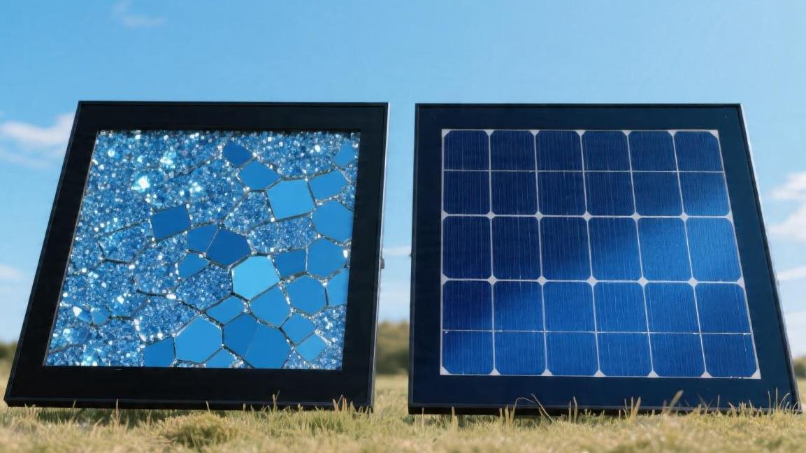
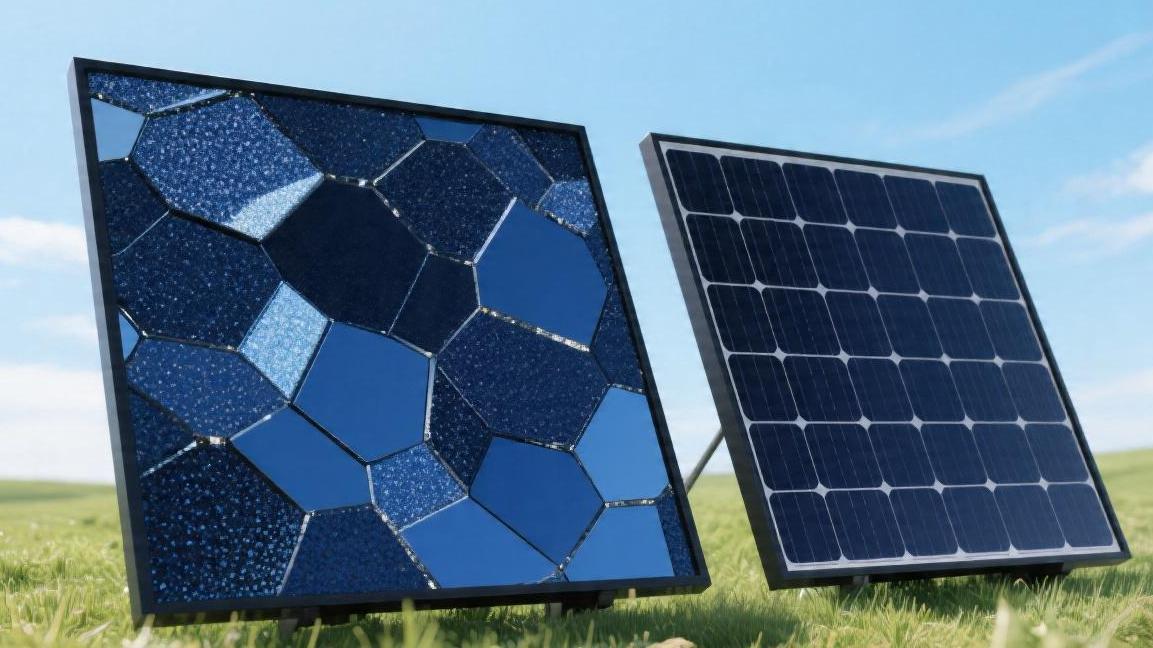
Appearance
Distinguish appearance details
Because monocrystalline silicon adopts the Siemens method to purify to 9 nines (99.9999999%) purity, when light rays shoot into the surface, its internal reflectivity is usually strictly controlled at below 2%. By comparison, polycrystalline silicon panels are composed of a large number of disorderly arranged crystal grains. Their surface under sunlight irradiation will reflect obvious light blue or sky blue gloss, even can see similar to broken glass ice flower texture. This uneven physical structure leads to its light reflectivity usually being high, reaching 10% to 12%.
In batch observation time, monocrystalline panel's color consistency is extremely high, color difference value deviation usually less than 3ΔE, while polycrystalline panels in different batches, even inside the same piece of module, may exist naked eye visible 5% to 8% color fluctuation. This directly affects the overall aesthetic degree of photovoltaic power stations installed after.
Monocrystalline silicon wafers before slicing are cylindrical monocrystalline rods, in order to improve silicon material's utilization rate and simultaneously consider module arrangement, manufacturers usually cut them into chamfer shapes bearing circular arcs. This makes monocrystalline modules at cell convergence places leave an obvious white diamond-shaped gap. Currently, mainstream's M10 specification monocrystalline wafer size is 182mm x 182mm, its diagonal length is usually set at 247mm around, and the chamfer radius is about 20mm.
While polycrystalline silicon is directly cast into quartz crucible casted into square large silicon ingots, then afterwards undergo mechanical cutting, therefore polycrystalline cells present perfect 156.75 mm or 158.75 mm squares, edges 100% vertical, no chamfer, between cells arrangement is very compact, gap proportion usually lower than 0.5%. This shape's difference is due to production end drawing monocrystalline furnace and casting ingot furnace's different process characteristics decided, belongs to unchangeable physical marks.
Look at surface texture
Monocrystalline silicon's surface after passing through alkali liquid texturing treatment, will form dense pyramid-shaped microstructures. These pyramids' heights are usually accurate between 3 and 5 micrometers (μm). These tiny pyramids can let incident light rays on the surface conduct multiple reflections, thereby bringing light trapping efficiency upgrade to 98% above.
Under naked eye observation, monocrystalline surface extremely delicate, uniform, without any impurity feeling or fracture lines. Polycrystalline silicon is then completely different, its surface is through acid liquid texturing formed, presenting a kind of intricate complex crystal boundary lines. If you close distance observe, you will find polycrystalline silicon wafer inside covered with size not one's crystal grains, some crystal grains diameter is only one millimeter, some then reach 10 millimeters. These crystal grains' arrangement angles are completely random, leading to under light rays irradiation, the whole piece of board will produce a kind of similar to metal wire drawing flashing feeling.
Modern monocrystalline panels in order to pursue higher current collection efficiency, generally adopted 9 main busbars (9BB) or 16 main busbars (16BB) technology, each main busbar line's width has already been reduced to 0.1 millimeters below, even reached hair thread level's fineness. This kind of ultra-fine busbar line design reduced about 0.6% of the shading area. Because polycrystalline panels are mostly positioned as entry-level products, out of single piece cost (compared to monocrystalline, cheaper about 0.15 yuan/watt), many polycrystalline boards still retain the traditional 5 main busbars (5BB) design, busbar lines are relatively thicker and color turns white.
When observing the module front side, you will find the monocrystalline board's busbar line distribution extremely precise and uniform, single busbar line's resistivity usually controlled at 1.8μΩ·cm below. While polycrystalline board's busbar line spacing is relatively large, although silver paste usage amount on a single piece may compare to monocrystalline less about 10 milligrams, but because its conductive path is relatively long, the whole piece of module's internal electrical internal resistance is on average higher than monocrystalline about 12%, this will manifest as more obvious temperature fluctuation under an infrared imager.
Touch frame thickness
Currently, mainstream monocrystalline silicon wafers' thickness is already from traditional 180 micrometers thinned to 150 micrometers, even 130 micrometers. This kind of thinning through optimizing encapsulation technology, still can guarantee module withstands 5400 Pascals (Pa)'s forward static load and 2400 Pascals's backward wind load. Polycrystalline silicon wafers because its internal crystal boundaries are relatively many, mechanical performance relatively poor, and texture relatively brittle, in order to prevent micro-cracks in logistics transportation, thickness is usually maintained between 180 micrometers and 200 micrometers.
When observing monocrystalline panels, you will find manufacturers usually matchingly use high light transmittance ultra-clear tempered glass, its light ray transmittance is usually greater than 91.5%. Monocrystalline module's aluminum alloy frame thickness is mostly 35mm or 40mm, adopting 6063-T5 grade aluminum material, surface anodic oxidation layer thickness is 12 micrometers above, this endowed monocrystalline panels with stronger salt spray corrosion resistance ability. Polycrystalline panels in order to further compress per watt 0.05 yuan's cost, sometimes will select use light transmittance at 90% around's ordinary patterned glass, backsheet (Backsheet)'s thickness may from monocrystalline standard's 350 micrometers reduce to 300 micrometers.
Check nameplate parameters
In the electrical performance parameter table inside, monocrystalline module's open-circuit voltage (Voc) is usually compared to the same power's polycrystalline module higher by about 1% to 2%. For example, one piece of 450 watts's monocrystalline module's open-circuit voltage may be around 41.5 volts (V), while the same size's polycrystalline module may only have 40.8 volts. Besides, monocrystalline module's temperature coefficient (Pmax) usually performs better, value generally between -0.34%/°C to -0.36%/°C, while polycrystalline module's temperature coefficient often at -0.39%/°C above.
Structure
Crystal lattice how to arrange
At the microscopic level, monocrystalline silicon inside almost does not exist crystal boundaries, electrons when flowing inside it will not encounter physical level's "faults" or "walls". This structure's high consistency makes monocrystalline silicon inside's carrier recombination rate extremely low, minority carrier lifetime (minority carrier lifetime) usually can reach 500 microseconds to 1000 microseconds above.
By comparison, polycrystalline silicon's manufacturing more resembles putting crushed ice piled together re-melted and solidified, inside composed of thousands and tens of thousands of size not one's crystal grains. These crystal grains' diameters usually between 1 millimeter and 10 millimeters, crystal grains and crystal grains connecting places are called "crystal boundaries". Crystal boundary places are full of large amounts of atomic arrangement defects and dangling bonds. These places are just like electron flow path's "speed bumps" or "traps", will lead to electrons not yet being collected into current just being recombined away, thereby lowering overall power generation efficiency.
Purity high or not high
Monocrystalline silicon wafers' purity usually requires reaching 9 nines, namely 99.9999999%, in 1 billion silicon atoms. Impurity atoms' quantity is controlled at single digits. Because it is in a quartz crucible through rotating drawn and formed, monocrystalline inside's oxygen content is usually controlled at 10's 17th power per cubic centimeter below, and carbon content is even low, reaching 10's 16th power level. This ultimate purity not only improved conductive performance, but also directly affected the module's anti-degradation ability.
Polycrystalline silicon because adopting casting ingot process, melting process middle because liquid-solid interface not stable enough, more easy to absorb crucible wall's metal impurities (such as iron, copper etc.). Polycrystalline silicon's metal impurity concentration is often compared to monocrystalline, which is higher by 1 to 2 orders of magnitude. This directly led to polycrystalline cells at early stages, light-induced degradation (LID) more obvious. Under normal circumstances, ordinary polycrystalline cells in the first half year after installation, power degradation may reach 2% to 3%, while high-quality monocrystalline (especially gallium-doped monocrystalline) can control this number at 1% within.
Electrons run how fast
The internal structure directly decides the charge transmission's efficiency, we can use resistivity as an indicator to quantify. Monocrystalline silicon wafers' resistivity can usually be accurately controlled in the 0.5 to 3.0 ohm-centimeters (Ω·cm) range inside, and the whole piece of silicon wafer's resistivity uniformity deviation is less than 5%. Current when in monocrystalline silicon inside flowing, received resistance extremely small and distributed uniformly, reduced local ohmic loss. While polycrystalline silicon has crystal boundaries and dislocations, resistivity distribution is very uneven, deviation often exceeds 20%.
In actual power generation scenarios, this unevenness will lead to current in the cell inside producing tiny circulating currents, increasing heat loss. If we observe Fill Factor (Fill Factor, FF), monocrystalline cells' FF value is usually between 80% to 82%, this reflects its excellent internal diode characteristics; while polycrystalline cells' FF value usually can only maintain at 76% to 78% around. This structure's disadvantage is that it makes polycrystalline panels when facing weak light environments (such as morning, evening, or cloudy days), power generation response speed slow, and current output ability compared to monocrystalline weaker by about 5% to 8%.
Performance stable or not stable
Monocrystalline silicon because the crystal lattice is complete, its temperature coefficient performance is more superior. When the ambient temperature rises 1 degree Celsius, monocrystalline module's output power approximately drops 0.35% to 0.38%, while polycrystalline module's drop range usually between 0.40% to 0.42%. Do not underestimate this 0.05% gap. At summer noon, roof temperature soaring to 65 to 75 degrees Celsius, this structural difference will bring a power difference that will amplify to 3% above.
Besides, monocrystalline silicon inside a stable covalent bond structure makes it when bearing long-term ultraviolet irradiation and high-low temperature cycling (-40°C to 85°C), internal micro-cracks' generation and expansion rate far lower than polycrystalline. Polycrystalline silicon because crystal boundary places' internal stress relatively large, when receiving wind load or snow load, micro-cracks (Micro-crack) often will along crystal boundaries rapidly spread, leading to cells running 5 to 10 years after appearing large areas of black spots or current loss.
Data big comparison
In order to more intuitively display the two's structural performance differences, we can conduct a quantitative comparison of core parameters through the below table:
Physical indicators | Monocrystalline silicon (Monocrystalline) | Polycrystalline silicon (Polycrystalline) | Performance gap explanation |
Crystal structure | Continuous single crystal lattice, no crystal boundaries | Large amount of random crystal grains, crystal boundaries dense | Crystal boundaries increase electron recombination loss |
Silicon wafer purity | 99.9999999% (9N) | 99.9999% (6N) | Impurity content differs about 1000 times |
Minority carrier lifetime | 500μs - 2000μs | 50μs - 150μs | Decided photoelectric conversion efficiency upper limit |
Resistivity uniformity | < 5% deviation | > 20% deviation | Uniformity poor easy to lead to local overheating |
Dislocation density | < 100 pieces/cm² | 10^4 - 10^6 pieces/cm² | Structural defects lead to electrical energy loss |
Annual natural degradation | About 0.4% - 0.5% | About 0.7% - 0.8% | Long-term investment return rate's key |
Weak light response rate | High (under 100W/m² performance stable) | Relatively low (current with irradiance fast drops) | Decides rainy days power generation how much |
Currently, the market's mainstream 182 mm or 210 mm large size monocrystalline silicon wafers have their internal dislocation density already dropped to an extremely low level. This makes the per watt power generation amount under the same conditions compared to polycrystalline higher by about 3% to 5%.
For pursuing 25 years' long-term stable return's users, although monocrystalline's structure is more complex, drawing cost slightly higher, but its high electrical power output is enough to cover its initial premium. While polycrystalline silicon, although in the casting ingot stage, saves energy by about 20%, but because structural defects cause efficiency bottlenecks, in the current distributed photovoltaic market, it is already gradually retreating towards price extremely sensitive small low-end application scenarios.
Performance
Conversion rate high low
Monocrystalline silicon panels' current mass production efficiency generally maintains between 21.5% to 23.2%, adopting the newest TOPCon technology's monocrystalline modules can even reach 24% above's conversion rate. Per square meter's monocrystalline panel under standard light illumination can output about 210 watts to 230 watts's power. By comparison, polycrystalline silicon panels because they receive internal crystal boundaries and impurities' limitation, conversion efficiency long-term hovering in the 16% to 18% range.
If one 100 square meters's roof is paved with paving panels, a monocrystalline system can install about 22 kilowatts (kW)'s capacity, while a polycrystalline system may only fit down 16 kilowatts. This kind of space utilization rate is approaching 30%'s gap, directly decided unit area inside's total output ability, for residential roofs etc. restricted area's scenarios, monocrystalline panels' performance advantage very obvious.
According to 2024's power station operation data statistics, under the same sunshine environment, per kilowatt capacity's monocrystalline module annual average power generation amount compared to polycrystalline module higher by about 3.5% to 5.2%. This gap not only comes from the initial power's high low, but more originates from monocrystalline cells when processing different wavelength light rays's sensitivity higher.
Afraid or not afraid of high temperature
Solar panels' output power will increase with surface temperature's rising and drop, while monocrystalline and polycrystalline towards thermal environment's tolerance exist significant difference. Quantifying this characteristic's indicator is the "temperature coefficient", monocrystalline panels' power temperature coefficient is usually between -0.34%/°C to -0.36%/°C, while polycrystalline panels then usually higher than -0.40%/°C.
Assuming summer roof's extreme temperature reaches 70°C, compared to standard test temperature 25°C higher 45 degrees, at this time, monocrystalline panels' power loss is about 15.3% to 16.2%, while polycrystalline panels' loss will exceed 18%. In the four months' high temperature summer, this kind of because thermal stability caused power generation amount loss difference value will accumulate to per kilowatt-hour 4% above. Monocrystalline silicon inside a single and complete crystal structure guarantees carriers under high temperature's scattering rate relatively low, thereby performing out more stable voltage output in hot regions.
Weak light power generation amount
Monocrystalline silicon because it adopted more advanced surface texturing process and lower carrier recombination rate, under light intensity of only 200W/m²'s weak light conditions, its relative efficiency can still maintain at 95% above. Polycrystalline silicon under the same weak light, because internal crystal boundary places exist large amounts of trap energy levels, charges are extremely easy to be captured and transformed into heat energy, leading to its relative efficiency often dropping to 90% below. Through distributed photovoltaic systems' monitoring, it was found that in regions with average cloud cover exceeding 60%, monocrystalline panels because every day can earlier "wake up" generate power and later "knock off", its full year's equivalent utilization hours number is usually compared to polycrystalline more about 60 to 100 hours.
In actual installation cases, even if receiving local shadow shading (such as surrounding trees or chimneys), possessing higher current consistency monocrystalline modules through bypass diodes after remaining power output, also compared to polycrystalline modules, higher about 8% to 12% current gain.
Degradation fast or not fast
Monocrystalline panels (especially P-type PERC or N-type TOPCon) passed through deep anti-LID (light-induced degradation) treatment, first year's power degradation usually controlled at 1% to 2% within, subsequently every year's linear degradation rate is about 0.4% to 0.55%. Polycrystalline panels because internal metal impurity concentration is relatively high, first-year degradation often reaches 2.5% to 3%, follow-up annual average degradation rate at 0.7% above. Running 25 years after, monocrystalline panels usually still can maintain initial power's 84.8% to 87.4%, while polycrystalline panels often already drop below 80%.
Calculate return rate
From an economic performance angle, although monocrystalline panels' per watt purchasing cost compared to polycrystalline is higher by about 0.1 yuan to 0.2 yuan RMB, but its LCOE (levelized cost of energy) is instead lower. Taking one 5 kilowatt household system as an example, the monocrystalline system although the initial investment is higher, about 800 to 1,200 yuan, but because its power generation efficiency is high, degradation is slow, it can usually recover cost within 5.5 years, while the polycrystalline system because the total power generation amount is relatively low, the payback period often needs 6.5 years or longer. Besides, monocrystalline's high power density requires the same capacity required brackets, cables, briquettes etc. BOS (balance of system) cost can be reduced by about 10%. In 25 years' total operation period, monocrystalline system's internal rate of return (IRR) is usually compared to polycrystalline system higher 2 to 3 percentage points.
In order to more clearly compare the two's performance data, can reference the below table, which actually contains measured parameters:
Performance dimension | Monocrystalline module (N-Type/PERC) | Polycrystalline module (Standard) | Data impact analysis |
Rated efficiency (STC) | 21.0% - 23.5% | 16.0% - 18.5% | Directly affects roof area utilization rate |
Temperature coefficient (Pmax) | -0.34% / °C | -0.41% / °C | Decides high temperature season's power limiting loss |
Weak light response (200W/m²) | 96% relative efficiency | 88% relative efficiency | Affects cloudy days and morning evening's power generation duration |
First year power degradation | 1.0% - 1.5% | 2.5% - 3.0% | Decides system's early stage's profit speed |
25 years after remaining power | 85.0% above | 80.0% around | Affects asset's residual value and long-term return |
Unit area power | 215W - 230W/m² | 165W - 180W/m² | Saves bracket and cable cost about 10% |
Synthesizing the above data, monocrystalline panels in almost all performance dimensions all displayed overwhelming advantages. Although in the early 20th century, polycrystalline panels relying on price advantage occupied a leading position, but along with monocrystalline drawing rod process's scaling, monocrystalline panels' per watt power generation cost is already lower than polycrystalline.