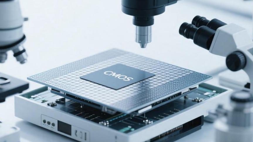
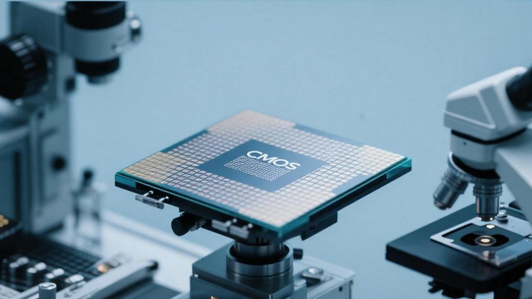
Why Is Polysilicon Used in CMOS | Conductivity, Reliability, Integration
Polysilicon in CMOS inside is widely used, mainly because of its good conductivity, reliability, and integration. Polysilicon has relatively low resistance, usually is tens to hundreds of ohms per centimeter, making current flow more efficient. In addition, polysilicon is suitable for large-scale integrated circuits, can be compatible with silicon base material, reduce cost and improve production efficiency.
Conductivity
How does electricity conduct?
Untreated pure polysilicon in 25℃ room temperature has a resistivity as high as 10's 5th power ohm-centimeters. The internal charge carrier concentration is only 1.5 times 10's 10th power pieces per cubic centimeter, belongs to the standard insulator level. Manufacturing 14 nanometers to 28 nanometers process's CMOS transistor time, engineers will use equipment to emit energy in 10 kiloelectron volts to 50 kiloelectron volts' high energy ion beam.
Through putting phosphorus ions or boron ions into a 150 nanometers thick polysilicon layer, the injection dose is usually precisely controlled at 10's 15th power to 10's 16th power pieces of atoms. Doped after's material Fermi level will happen 0.5 electron volts to 0.7 electron volts' physical shift. Completing the above process, the N-type polysilicon inside's free electron concentration will violently increase to per cubic centimeter 10's 19th power to 10's 20th power pieces level.
As high as 10 magnitude orders' concentration leap, makes polysilicon's overall conductivity performance improve 1 million times above. Compared to 300 millimeters wafer substrate's single crystal structure, thickness error controlled in plus minus 5% inside the polysilicon thin layer is able to bear per square centimeter 10's 5th power amperes' high density continuous current.
Grain boundary block road
Polysilicon thin film by thousands and tens of thousands of pieces, dimension in 100 nanometers to 500 nanometers, varying small crystal grains spliced to become. Crystal grain and crystal grain meeting's junction place exists density as high as per square centimeter 10's 12th power pieces above's defect traps. Applied's test voltage in the 1.2-volt to 3.3-volt interval fluctuates over time, about 30% to 40% of free moving charge will be by grain boundary place's potential barrier wall forcibly blocked. This potential barrier's physical height is roughly 0.05 volts to 0.1 volts, causing the polysilicon inside's electron moving rate to be only per volt-second 10 to 50 square centimeters.
In order to offset potential barrier brought by 50%'s conductivity serious loss, doped atom's injection quantity must be high to per cubic centimeter 5 times 10's 19th power pieces above's limited threshold value. Impurity concentration breaks through critical point after, potential barrier height will with 90% ratio rapidly reduce, blocking width also will shrink to 2 nanometers inside. At this time, the electron penetration probability recovered 80%, and the overall material's resistivity dropped to 0.001 ohm-centimeters, good conductor qualified interval.
Lower resistance
Passing large dose ion injection after, originally sheet resistance as high as per square 10's 8th power ohms' polysilicon, sheet resistance index will large magnitude drop to per square 10 ohms to 30 ohms' range. In clock frequency reaches 2.5 gigahertz, the high-speed calculation chip inside needs research and development personnel to signal propagation's RC delay time rigidly compress to 20 picoseconds below.
· Adopting chemical vapor deposition process grown's 200 nanometers thickness polysilicon, surface roughness maintains in root mean square value 0.5 nanometers' extremely low level.
· In order to further sheet resistance to low 70%, polysilicon will top deposit a layer thickness of about 15 nanometers to 25 nanometers' pure titanium or pure cobalt metal.
· Passing 500℃ to 700℃'s high temperature chemical reaction, generated's silicide can final's sheet resistance lower to per square 1 ohm to 5 ohms.
· Resistance value completes lowering after, by gate metal wiring triggered's dynamic power consumption dropped about 15% to 20%, signal end to end's transmission speed improved at least 3 times.
· Polysilicon and silicide's composite conductive structure yield rate, after experiencing 100 thousand times electrification cycle pressure test, still keeps in 99.9%'s extremely high standard.
Depletion layer trouble
Manufacturing gate dimension shrinks to 90 nanometers below specification time, polysilicon near silicon dioxide insulation layer about 1 nanometer to 2 nanometers' microscopic area will appear charge carrier concentration sudden drop's physical phenomenon. In 1.0 volts' forward bias working voltage driving under, this area's active charge carrier will be repelled, causing the actual equivalent oxide thickness to passively increase from 0.3 nanometers to 0.5 nanometers.
· Because the gate layer's equivalent physical thickness increased 20% to 30%, the transistor's overall gate capacitance capacity will along with it lose 10% to 15%.
· Capacitance capacity drop brought's 30 milliseconds inside associated reaction is, source to drain's maximum driving current output reduced 5% to 8%.
· The process team must forcibly push the local doping concentration of the polysilicon bottom to per cubic centimeter 10's 20th power pieces atoms' material limit numerical value.
· Increasing 60% heavy doping dose after, the depletion layer's physical thickness is forcibly compressed to 0.5 nanometers' safe threshold value below.
· High intensity injection prevent depletion scheme makes single piece 200 square millimeters area chip's leakage current numerical value, stably maintains at 50 nanoamperes inside the factory qualified line.
High temperature bake a bake
Normal temperature under hit into polysilicon inside's ions have about 80% to 90% initially in the non-activated state, did not produce provide 1 extra electron or hole's actual conductive function. Completed processing's wafer must be sent into rapid thermal annealing equipment, in a 1000℃ to 1050℃ extremely high furnace temperature, under bake 10 seconds to 30 seconds' time.
· Annealing furnace inside's environmental temperature every rises 50℃, impurity atom's crystal lattice replacement rate then will exponentially increase nearly 2.5 times.
· Complete's 30-second heating cycle inside, 95% of phosphorus atoms or boron atoms will happen 0.5 nanometers to 1.5 nanometers' displacement, accurately stuck into silicon atom's standard crystal lattice position.
· Activation process's total thermal budget receives extremely strict control, impurity atom's horizontal accidental diffusion distance must be controlled in 10 nanometers' stipulated upper limit inside.
· Heating step completes after, annealing equipment with per second 50℃ to 100℃'s cooling rate rapidly cools, prevents as high as 10's 20th power times concentration's impurity in 3 seconds inside happens secondary precipitation.
· Completely heat activated after's polysilicon thin film possesses as long as 10 years above's conductive stability, daily resistance fluctuation rate in 85℃'s aging baking test inside lower than 2%.
Reliability
Can withstand heat
Polysilicon in physical characteristics possesses 1414℃'s high melting point, and in the later stage of chip manufacturing's heat treatment stage provides extremely large temperature tolerance. In the front-end process inside, in order to repair ion injection brought's crystal lattice damage, the wafer needs to be annealed in an annealing furnace inside to withstand as high as 1000℃ to 1050℃'s high temperature baking, continuous time reaches 10 seconds to 30 seconds.
Polysilicon in this temperature interval inside maintains a solid state's physical structure, completely avoiding metal material in the same condition under possible melting deformation. Polysilicon's thermal expansion coefficient is about 2.8 times 10's negative 6th power per Kelvin, with the bottom layer single crystal silicon substrate's 2.6 times 10's negative 6th power highly fitting. In passing as many as 20 times' 500℃ to 1000℃'s heating cooling cycle after, the gate material and insulation layer between due to thermal expansion and cold contraction generated's physical shear stress is limited to 50 megapascals inside.
· Conventional metal aluminum in 660℃ then will happen liquefaction phase change. If adopting aluminum as a gate, the whole CMOS's manufacturing thermal budget upper limit is dead dead limited to the 450℃ to 500℃ low temperature interval.
· Situated at 450℃ low temperature environment, injected's impurity atom activation rate lacks 20%, causes source and drain's contact resistance to maintain in per square micrometer 1000 ohms above's exceeding standard state.
· Polysilicon and surrounding silicon dioxide insulation layer's thermal expansion coefficient difference value is less than 15%, withstanding 125℃'s high intensity continuous electrification running 100 thousand hours after, physical peeling probability low to 0.001%.
· Annealing furnace with per minute 75℃'s rate rapidly heats up time, polysilicon thin film inside generated's thermal stress is able to towards surrounding evenly disperse, effectively suppressed length greater than 0.1 micrometers' physical crack generation.
Interface not cause trouble
Polysilicon deposited in thickness only is 2 nanometers to 5 nanometers' silicon dioxide ultra-thin insulation layer above time, presents extremely high chemical inertness and crystal lattice matching degree. In applying 1.5 volts to 3.3 volts' gate bias working voltage time, polysilicon and insulation layer junction place's interface state defect density strictly maintains in per square centimeter 10's 10th power pieces electron volts negative 1st power's extremely low level.
Ordinary metal material in contact with silicon dioxide time, will in 400℃ above's process environment inside happen oxidation reduction reaction, snatch silicon dioxide inside's oxygen atoms, generate thickness uneven's oxidized metal layer and towards below silicon substrate release free silicon atoms. Polysilicon itself, namely, is the silicon element, and in an environment as high as 1050℃'s will not happen destructive chemical reactions with silicon dioxide.
Test parameter | Polysilicon gate structure | Traditional aluminum gate structure |
Physical melting point limit | 1414℃ | 660℃ |
Interface state defect density | Less than 1x10's 10th power/cm² | Greater than 5x10's 11th power/cm² |
High temperature chemical stability | 1050℃ under no reaction | 500℃ happens oxidation-reduction reaction |
Linear thermal expansion coefficient | 2.8 x 10's negative 6th power (1/K) | 23.1 x 10's negative 6th power (1/K) |
Anti-electromigration threshold | Greater than 10's 7th power A/cm² | About 10's 5th power A/cm² |
Prevent electrical penetration
In 28 nanometers and more advanced process nodes, the gate oxide layer's physical thickness is compressed to 2 nanometers around, and the internal withstands electric field intensity as high as per centimeter 5 megavolts to 10 megavolts. In such extreme electric field pressure, the material inside the atomic nucleus and the electron's binding force face a huge test.
The electromigration effect is a common reason for chip physical scrapping, when current density breaks through per square centimeter 10's 5th power amperes times, metal atoms will be by high speed moving electrons hit to generate physical displacement, eventually in wiring or gate inside form width exceeding 50 nanometers' microscopic physical voids. Polysilicon inside by covalent bonds bind, atom arrangement's binding energy far higher than ordinary metal's metallic bond.
· Applying per square centimeter 10's 6th power amperes' limit test current density time, polysilicon inside happen electromigration's probability not reach one thousandth, physical structure maintain time exceeds 50 thousand hours.
· In 125℃ environmental temperature under continuously applying 1.2 times rated working voltage, polysilicon gate and insulation layer combination's time dependent dielectric breakdown (TDDB) life estimated exceeds 15 years.
· Because polysilicon work function is 4.0 to 5.2 electron volts, it is adjustable, able to precisely match the bottom layer silicon channel's energy band structure, eliminated insulation layer two ends about 0.3 electron volts' invalid potential barrier voltage drop.
· Gate leakage current in 25℃ standard test temperature under is dead dead suppressed in per square micrometer 10 picoamperes to 50 picoamperes' qualified range, exempted 95%'s invalid static power consumption heating phenomenon.
Anti-aging strong
Take channel length only has 28 nanometers' N-type transistor as an example. Drain apply 1.0 volts' voltage after, source to drain between narrow area's electric field intensity surges. Part electrons in a horizontal electric field inside obtain as high as 1.5 electron volts to 2.0 electron volts' huge kinetic energy, upgrade become “hot electrons”.
High energy hot electrons will break through the potential barrier shield and rush into the gate insulation layer inside, be forcibly captured by dangling bonds at the interface place, and form a fixed negative charge. Polysilicon's uniform microscopic crystal grain structure, and lower than per square centimeter 10's 11th power pieces' internal defect quantity, large magnitude lowered trap capture charge's probability.
· In negative bias temperature instability (NBTI) special test, towards the test piece apply a negative 1.2 volts' bias voltage and will environmental temperature pull up to 125℃, continuously apply pressure for 1000 hours.
· Passing limit high voltage high temperature double torture, polysilicon P-type MOS tube's threshold voltage absolute shift amount is limited to 30 millivolts to 50 millivolts' extremely small interval inside.
· If material threshold voltage drift exceeds 100 millivolts, it will cause the whole logic circuit's high-low level flip time delay to exceed 50 picoseconds, triggering overall calculation's timing confusion.
· Polysilicon gate excellent's anti charge capture ability, makes transistor experiencing as high as 10's 12th power times' high low level switch after, transconductance degradation rate controlled in 5% to 8%'s safe boundary inside.
Integration
Spread film output high
Chip foundry factory in 300 millimeters (12 inches) wafer production line inside, adopts low pressure chemical vapor deposition (LPCVD) equipment to conduct thin film growth. The operator will 100 pieces to 150 pieces bare wafers simultaneously send into a huge quartz furnace tube inside, will furnace cavity inside's working air pressure precisely extract and maintain in 0.2 torr to 1.0 torr's extremely low vacuum state. Pass into high purity's silane (SiH4) gas after, equipment will environmental temperature strictly stabilize in 580℃ to 650℃'s interval.
Silane gas in high temperature surface happens thermal decomposition reaction, with per minute 10 nanometers to 20 nanometers' constant rate in silicon wafer surface deposit out solid state's polysilicon thin film. The whole furnace processing cycle usually consumes time of about 120 minutes to 150 minutes, a single time task, then can output exceeding 100 pieces of thickness 150 nanometers' standard wafers.
The same one-piece area about 70 thousand square millimeters' wafer surface, polysilicon thickness's physical error is forcibly compressed in a plus minus 2% extremely small fluctuation range inside. Per square centimeter's surface particle defect quantity lower than 0.05 pieces, guaranteed subsequent hundreds courses' lithography process's yield rate base number.
Single unit LPCVD equipment's full load running throughput capacity is able to reach per hour 50 pieces to 70 pieces wafers, compared to every time only being able to process a single piece wafer's atomic layer deposition (ALD) machine tool, polysilicon's single step production efficiency pulled high about 40 times to 50 times, large magnitude diluted single piece wafer's machine tool depreciation expense.
Position align accurate
Lithography machine will polysilicon gate engrave shape after, ion injection machine emits energy as high as 50 kiloelectron volts to 100 kiloelectron volts' arsenic ions or phosphorus ion beam. As high as per square centimeter 10's 15th power pieces of impurity atoms will vertically bombard the wafer surface, polysilicon gate completely blocked below the channel area's ion penetration, let impurity only fall precisely into the exposed source drain area.
Originally adopting metal aluminum coordinating old style lithography alignment time, physical dislocation deviation often reaches 0.5 micrometers to 1.0 micrometers, forcing designers to reserve width reach 1.2 micrometers' redundant overlap area. Polysilicon baffle eliminated as high as 100%'s human alignment error, will gate and source drain between's parasitic overlap area shrink to not reach 5 nanometers.
Parasitic overlap capacitance's physical capacity cliff style dropped about 60% to 75%, transistor conducting high low level flip's RC delay time from 500 picoseconds sharply reduced to 10 picoseconds to 20 picoseconds' interval, single piece chip's highest clock calculation frequency from 50 megahertz easily crossed to 2.5 gigahertz above's level.
Easy cut and easy engrave
Engineers towards etching cavity body inside inject flow rate is per minute 50 standard cubic centimeters to 100 standard cubic centimeters' chlorine gas (Cl2) or carbon tetrafluoride (CF4) etc. halogen-containing gas, and apply 13.56 megahertz's radio frequency power source to excite high density plasma. Plasma concentration reaches per cubic centimeter 10's 11th power pieces' level time, fluorine-based or chlorine-based free radicals will with polysilicon happen violent's anisotropic chemical reaction, generate silicon tetrachloride etc. Volatile gases can be extracted away by vacuum pump.
Polysilicon towards bottom layer silicon dioxide insulation material's etching selectivity ratio is as high as 50 to 1, even 100 to 1. Strong plasma beam cutting through 150 nanometers thickness's polysilicon layer after, once touching the bottom layer only has 2 nanometers thick's silicon dioxide, etching rate will suddenly drop 98% above.
Extremely high material selectivity ratio makes etching line's sidewall verticality maintain in 88 degrees to 92 degrees' perfect right angle interval, line width's physical loss amount (CD Loss) strictly controlled in 1 nanometer to 2 nanometers' allowed error inside, completely avoided towards bottom layer extremely thin oxide layer's excessive physical penetration destruction.
Budget extremely cost-effective
A strip monthly capacity reaches 50 thousand pieces of wafers' standardized 28 nanometers chip assembly line, machine tool procurement and daily maintenance's fund consumption amount is extremely huge. Procuring a unit mature's polysilicon LPCVD deposition system, hardware price roughly in 1.5 million US dollars to 2.5 million US dollars, full load running's equipment mean time between failures (MTBF) usually as long as 5000 hours above.
Contrast under, later stage high-K metal gate (HKMG) process needed's ultra-high vacuum atomic layer deposition (ALD) equipment, single unit procurement budget as high as 5 million US dollars to 8 million US dollars, and daily consumable expenditure increased about 300% to 400%. In the polysilicon process route, waste piece scrap rate year-round maintains at 0.05% below's extremely low standard, 12-inch wafer's comprehensive yield rate stabilizes at 98.5% to 99.5% between.