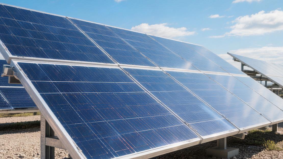
What are the characteristics of the most efficient solar panels
Currently, the most efficient solar panels generally adopt N-type monocrystalline silicon technology, with photoelectric conversion efficiency as high as 22% to 24% or more.
They possess three core characteristics: first, power attenuation is extremely low, with first-year attenuation usually less than 1%, ensuring stable high output for more than 25 years;
Second, they have an excellent temperature coefficient (approximately -0.26%/℃), maintaining high power generation efficiency even on hot summer days and avoiding performance degradation caused by heat;
Third, they mostly combine half-cut and multi-busbar designs, which effectively reduces internal resistance and minimizes power loss caused by shadow occlusion.
Advanced Cell Material
Phosphorus Doping
Phosphorus atoms are injected into the N-type monocrystalline silicon substrate during the crystal pulling process, reaching a free electron concentration inside the silicon wafer of the magnitude of 10^15 to 10^16 cm^-3.
After replacing the conventional boron doping process, the light-induced degradation phenomenon in the first year caused by boron-oxygen complexes is eliminated, and the power loss rate of the module in the first year of operation is limited to between 0.8% and 1.0%.
In the production stage of tunnel oxide passivated contact, the manufacturing process deposits an extremely thin silicon dioxide tunneling layer with a thickness of 1.5 to 2.0 nanometers on the back of the silicon wafer, followed by a layer of 15 to 20 nanometers of doped polysilicon thin film.
Electrons rely on the quantum tunneling effect to cross the silicon dioxide barrier of less than 2 nanometers in thickness, while minority carrier holes are completely blocked outside the interface, causing the surface recombination velocity to drop sharply below 10 cm/s.
The open-circuit voltage of the panel crosses the theoretical limit of 720 millivolts and stabilizes at around 732 millivolts.
· The physical thickness of the silicon wafer has been compressed from 160 microns to 130 microns, corresponding to a reduction in silicon material consumption per watt to 2.4 grams.
· For a standard 72-cell panel with an area of 2.58 square meters, the photoelectric conversion efficiency in a mass production environment is in the range of 22.5% to 22.8%, and the actual measured maximum output power falls within the range of 570 watts to 590 watts.
Using Heterojunction
Heterojunction cells deposit intrinsic amorphous silicon thin films and doped amorphous silicon thin films with a thickness of 5 to 10 nanometers on the front and back sides of the N-type silicon substrate, respectively.
Amorphous silicon material has a bandgap width of 1.7 electron volts, which, combined with 1.12 electron volts of crystalline silicon, expands the spectral absorption range of the panel from a narrow frequency to the full band of 300 to 1,100 nanometers.
The completely symmetrical double-sided deposition structure grants the panel extremely high bifacial gain capability, with a bifaciality parameter as high as 85% to 90%.
The furnace temperature throughout the entire production process is strictly controlled below 200℃, eliminating lattice thermal stress damage caused by high-temperature baking, and maintaining a production line yield rate of 98.5%.
· When the module is installed on a flat concrete roof with a reflectivity of 30%, the back side can absorb approximately 300 watts of reflected radiation per square meter, which translates to an increase of 9% to 12% in actual power generation for the overall system.
· The power temperature coefficient of the panel is extremely low, remaining in the range of -0.24%/℃ to -0.26%/℃. In desert areas where the ambient temperature rises to 75℃, the internal thermal loss of the panel is 15 to 20 watts less than that of ordinary models.
Fully Flat Back Surface
Back contact technology transfers all positive and negative metal grid lines from both the front and back sides to the back of the cell, achieving 100% physical exposure of the light-receiving surface without any silver paste lines blocking the incident light.
The main busbars and fine grids on the front of conventional panels reflect and block 2.5% to 3% of sunlight; after eliminating physical blockage, the short-circuit current density increases by 1.5 to 2.0 mA/cm^2.
The metal electrodes on the back are arranged in a comb-like interlocking pattern, with the widths of the P+ doped region and N+ doped region set to 300 microns and 800 microns, respectively.
Since the physical distance between the positive and negative electrodes on the back is only a few dozen microns, the leakage rate at the edge of the PN junction is forcibly controlled at the microampere level of 10^-8 amperes.
· The back electrodes do not need to consider light transmittance, and their thickness has been increased from the conventional 5 microns to 15 to 20 microns, significantly reducing internal transmission resistivity by 30%. The reduction in series resistance pulls the fill factor of the panel up to 83% to 85%.
· A mass-produced panel with an area of approximately 2 square meters has a single-unit rated power calibrated between 460 watts and 475 watts.
Perovskite Tandem
Tandem cells made by stacking crystalline silicon and perovskite materials break through the theoretical conversion limit of 29.4% for single-junction silicon cells.
The top perovskite layer specifically absorbs high-energy short-wave blue-green light in the wavelength range of 300 to 800 nanometers, with the bandgap width precisely adjusted to 1.65 to 1.75 electron volts through chemical stoichiometry.
The bottom silicon-based layer is responsible for absorbing low-energy infrared light with wavelengths from 800 to 1,200 nanometers.
The physical mechanism of frequency-segmented spectrum absorption pushes the upper limit of conversion efficiency to 43%.
The material is extremely sensitive to humidity; under conditions where the relative humidity exceeds 40% or continuous exposure to an 85℃ environment reaches 1,000 hours, the crystal structure will undergo a phase change, causing an efficiency drop of more than 10%.
Panel encapsulation must use POE polymer transparent adhesive film with a water vapor transmission rate lower than 10^-4 g/m^2·day for double-layer water-blocking pressing.
· Under a standard test size of 1 square centimeter, the certified efficiency of the heterojunction tandem cell reaches 33.9%.
· The actual thickness of the perovskite coating is only 500 to 800 nanometers, accounting for only one-fourth of the thickness of a monocrystalline silicon wafer, with material consumption per square meter of panel being less than 1 gram.
Cutting-Edge Architectures
Cut in Half
Using a 1064 nm wavelength infrared non-destructive laser scribing equipment assisted by a -150℃ cooling spray, two rectangular sub-cells of exactly equal size are precisely cut along the center line of a complete monocrystalline silicon wafer with a side length of 182 mm or 210 mm.
Physical cutting causes the rated operating current inside a single cell to decrease from the original 13.5 amperes to 6.75 amperes.
According to the derivation of Joule's Law in physics, the reduction of internal current by half causes the internal resistance thermal loss of the module in the series circuit to drop sharply by 75% in the mathematical model.
In a rooftop test scenario exposed to scorching summer sun with the ambient temperature rising to 45℃, the actual operating surface temperature of the panel drops from the usual 68℃ to 65℃.
For every 3℃ decrease in temperature, calculated according to the power temperature coefficient of -0.28%/℃, the output terminal can retain an additional 0.84% of the rated power, which translates into significant power generation gains over a 25-year life cycle.
A 144-cell half-cut structure module is configured with three sets of parallel bypass diodes. When the lower half of the panel is completely blocked by a 40 cm wide chimney shadow, the 72 independent sub-circuits in the upper half still maintain a current output of 3.37 amperes, maintaining 50% or 220 watts of available power generation, avoiding the risk of power failure where a full-cell module would drop to 0 watts under the same blockage.
Shingled Layout
Flexible conductive adhesive is used to replace traditional lead-tin alloy solder strips, laying the edges of the cell strips, cut into 5 to 6 narrow strips, in an overlapping manner. The physical width of the overlap is precisely set in the range of 1.2 mm to 1.5 mm.
This completely eliminates the average 2 mm mechanical gap between cells in traditional arrays. Within a standard panel frame with a length and width of 1996 mm and 1,092 mm, respectively, the proportion of the active light-receiving area has increased from the conventional 93% to 97.5%.
The conductive adhesive contains 75% to 80% nano-silver particles. After undergoing a 15-minute thermal curing process in a laminator at 160℃, a flexible connection layer with an extremely low contact resistance of 0.005 ohms is formed.
When the panel surface bears a uniform static snow load of 5400 Pascals, the flexible adhesive layer can absorb and buffer a downward mechanical deformation of 30 mm, greatly reducing the probability of micro-cracks caused by cell fracture by 60%.
After eliminating the physical blockage of metal solder ribbons on the front, the short-circuit current increased by 0.4 to 0.6 amperes under standard test conditions. By filling the internal space of a 60-cell full-size module with 65 equivalent shingled cells, the output power under the same external dimensions jumped from 380 watts to 415 watts, and the photoelectric conversion density per unit area reached 210 watts per square meter.
Covered with Fine Wires
In the screen printing process of the front of the cell, 4 to 5 flat main busbars with a width of 0.7 mm were abandoned in favor of 9 to 16 cylindrical micro-wires with a diameter of only 0.26 mm to 0.30 mm.
The optical refraction characteristics of the cylindrical surface can redirect 75% to 80% of the incident light hitting the wires back to the silicon wafer surface covered with a silicon nitride anti-reflective film, forming a secondary optical absorption mechanism.
The thin and dense distribution of wires shortens the physical distance for electrons to move within the silicon substrate to the collection electrode to less than 1.1 mm.
The reduction in series resistance pulls the fill factor of the panel up from 79% to 82.5%.
The consumption of front silver paste in the screen printing stage was reduced from 110 mg per cell to 75 mg, and the manufacturing cost of metallization consumables for a single cell subsequently dropped by 15%.
The dense micro-wire network builds extremely redundant current transmission channels. When a silicon wafer encounters an external impact that produces a microscopic crack with a length of 5 mm and a width of 0.1 mm, electrons can quickly bypass it along adjacent healthy wires with a spacing of only 1.5 mm. The overall power loss of the module is forcibly limited to within 0.2%, ensuring the stability of long-term output.
Extremely Tight Tiling
High-density encapsulation technology, while retaining traditional round solder ribbons, utilizes reflective ribbons with triangular micro-structures and a special flattening process to compress the physical gap between cells to a limit of 0.5 mm, or uses elastic ribbons to achieve a small negative gap overlap of 0.2 mm.
The displacement accuracy of the robotic arms on the assembly line is strictly calibrated within a tolerance range of plus or minus 0.05 mm, ensuring that arrays connected in series from 210 mm large-size silicon wafers do not undergo millimeter-level cumulative misalignment on a 2.3-meter-long backsheet.
The blank area inside the panel has been reduced by nearly 80%, and the encapsulation loss rate has dropped significantly from 1.5% to 0.2%.
For 78-cell ultra-large format panels, the operating voltage is stable at 45.3 volts, and the short-circuit current has climbed to 18.5 amperes.
The accompanying junction box is filled with flame-retardant silicone with a thermal conductivity of 1.2 W/m·K to handle high-current conditions.
Under standard air mass AM1.5 and 1,000 W/m^2 laboratory light source vertical irradiation, the array using high-density seamless splicing can maximize the effective light-emitting area, allowing the overall photoelectric conversion efficiency of the highest mass-produced modules to steadily step onto the 22.3% platform, and the peak power of a single panel has crossed the industrial threshold of 670 watts.
Low Temperature Coefficient
Withstanding High Temperatures
Standard testing conditions for solar panels are set at a laboratory environment of 25℃, an irradiance of 1,000 W/m^2, and an air mass of AM1.5.
In actual outdoor environments in July or August, the surface temperature of panels installed on asphalt roofs often climbs to the 65℃ to 70℃ range.
The temperature deviation between actual operation and the laboratory reaches a range of 40℃ to 45℃.
For every 1℃ increase in cell temperature, the output power drops by a specific percentage, defined in physics as the maximum power temperature coefficient.
The temperature coefficient indicators for older generation polycrystalline silicon panels usually hover between -0.40%/℃ and -0.45%/℃.
At an operating temperature of 65℃, a panel rated at 400 watts will suffer a power loss as high as 16%, equivalent to 64 watts evaporating, with the actual output leaving only 336 watts.
The most efficient N-type panels strictly suppress this temperature coefficient to between -0.24%/℃ and -0.28%/℃.
Under the same 65℃ high-temperature baking, the power reduction rate is limited to 9.6% to 11.2%, and the panel can still maintain an output capability of 355 watts to 361 watts.
Taking 1000 panels as a test sample, when the ambient temperature is pushed to 65℃, the variance of the power attenuation distribution from high-frequency sampling is controlled within 0.02, and the median attenuation rate stays precisely at the 10.5% scale.
· A 5% power difference translates to 1000 W/m^2 of sunlight, equivalent to squeezing out an extra 50 watts of rated output per square meter of area.
· For a 10 kW home rooftop system running at full load for 5 hours at noon during high temperatures, low temperature coefficient panels can produce an extra 2.5 kWh of physical electricity daily.
Stabilizing High Voltage
When the ambient temperature rises, the 1.12 electron volt bandgap width of silicon material undergoes micrometer-level contraction, and the intrinsic carrier concentration subsequently shows exponential growth.
Thermodynamic changes cause the open-circuit voltage to drop significantly at a rate of -0.25% to -0.30% per degree Celsius.
Although the short-circuit current will rise slightly with a small amplitude of +0.04% to +0.05%/℃, a few dozen milliamperes of current increase cannot compensate for the huge loss of several volts at the voltage terminal.
Efficient cells keep the voltage decay rate strictly at the -0.22%/℃ standard line by increasing the substrate doping concentration to the magnitude of 10^16 cm^-3 and optimizing surface passivation processes to lower the reverse saturation current density to a microampere level of 10^-14 A/cm^2.
During a continuous high-temperature test cycle of three months, the standard deviation of open-circuit voltage fluctuations was compressed below 0.1 volts, ensuring that the frequency of the inverter tracking the maximum power point is stable at 50 times per second.
· When the panel is under an extreme thermal load of 75℃, high-efficiency cells with a standard voltage of 42.5 volts can stabilize the working voltage above 38.6 volts, ensuring the inverter always operates within the highest conversion efficiency range of 35 volts to 45 volts.
· The fill factor, which measures the fullness of the current-voltage curve, usually drops from 82% to 78% under thermal stress, but the extremely low series resistance variance forces the value to stay above 80%.
Thin Films Can Reduce Temperature
Depositing intrinsic and doped amorphous silicon thin films with a thickness of only 5 to 10 nanometers on an N-type crystalline silicon substrate builds a heterojunction physical form that fundamentally reshapes the panel's thermal response curve.
The amorphous silicon layer with a wide bandgap of 1.7 electron volts can provide a stronger built-in electric field, pushing the initial open-circuit voltage of the cell from a conventional 680 millivolts to a peak of 730 to 750 millivolts.
The larger denominator of the initial voltage greatly dilutes the percentage of voltage attenuation caused by temperature rise in mathematical ratios.
In the IEC 61,215 standard thermal cycle test chamber, the panel repeatedly undergoes 200 cycles within a temperature range of -40℃ to +85℃. The power degradation rate of the heterojunction structure remains below the limit of 1.5%, much lower than the 2.5% to 3.0% degradation probability of traditional structures.
· In desert demonstration bases where the annual average temperature exceeds 35℃ and the ground sand temperature breaks 80℃, the actual operating temperature of high-efficiency panels is generally 2℃ to 3℃ lower than ordinary models. The symmetrical thin-film structure has an infrared emissivity of 0.85, allowing more waste heat to be radiated back into the air.
· The specific heat capacity of a module containing 3.2 mm tempered glass and POE film limits the rate of instantaneous temperature rise of the panel to a low speed of 0.5℃ per minute under sudden irradiation of 1,200 W/m^2.
Generating More Power in Summer
Placing the low temperature coefficient into a 25-year life cycle financial calculation model shows quantified statistical data on the boost effect for the Levelized Cost of Energy (LCOE) and the Internal Rate of Return (IRR).
Using a 50 MW ground power plant located in a tropical savanna climate zone as a statistical sample, the number of days with a maximum daytime temperature exceeding 32℃ is as many as 180 days.
Comparing panels with a -0.26%/℃ coefficient to those with a -0.35%/℃ coefficient, the actual power generation efficiency recorded a net increase of 3.5% to 4.2% during the peak high-temperature load from 11 AM to 3 PM.
Running a regression analysis based on 1800 effective utilization hours per year, this temperature deviation characteristic can yield an extra 75,000 to 90,000 kWh of electricity per megawatt of installed capacity annually.
· Within a 300-month operation cycle, assuming the average annual linear attenuation rate of modules is set at 0.4%, a 50 MW power plant will generate more than 110 million extra kWh of electricity. At an on-grid settlement price of 0.05 USD per kWh, this can generate an additional 5.5 million USD in monetary return.
· The overall system LCOE drops from 0.035 USD/kWh to 0.033 USD/kWh, pushing the project's internal rate of return from a baseline of 8.5% up to 9.2%, and the static investment recovery period is shortened by 7 to 9 months on the timeline.