What's New in Solar Cell Materials | Perovskites, Tandems, Flexibility
Perovskite cell efficiency has already exceeded 25%, tandem batteries have broken through 30%, flexible module thickness can be as low as 1 mm, suitable for curved surface installation, in actual application need control humidity lower than 40% and add encapsulation layer to improve stability.
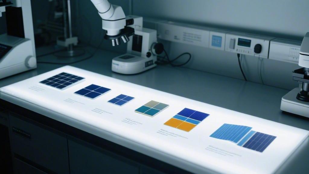
Perovskites
How Materials Grow
Light-absorbing materials follow the octahedral crystal structure with the general formula ABX3, A-site occupies the cubic unit cell's vertex position, filled by methylammonium ion or formamidinium ion with crystal radius between 1.6 Angstroms to 2.5 Angstroms. The B-site is at the unit cell body center, mostly as divalent lead ion or tin ion with a radius of 1.19 Angstroms. X-site distributed in 6 face-center positions, composed of iodine ion, bromine ion, or chlorine ion with a radius of 1.96 Angstroms to 2.20 Angstroms.
Material R&D personnel through adjusting the X-site iodine atom and bromine atom's molar mixing ratio, can take its optical absorption bandgap from 1.48 electron volts smoothly adjust to 2.30 electron volts. Precise bandgap adjustment lets material's absorption spectrum edge extend from 800 nanometers to 540 nanometers, matching different solar spectrum frequency bands' photon energy. During the crystallization process, lead halide octahedra through corner-sharing way in three-dimensional space within infinitely extend, forming microscopic architecture with lattice constants of about 6.28 Angstroms to 6.35 Angstroms.
How Coating Brushed
Producing 0.5 micron thick standard light-absorbing layer no longer relies on 1400 degrees Celsius high temperature smelting equipment, manufacturing whole process environment temperature controlled between 100 degrees Celsius to 150 degrees Celsius.
· Factory adopts slot-die coating equipment, taking dimethylformamide and dimethyl sulfoxide mixed solution dissolved with precursor powder squeezed onto conductive glass substrate, coating speed maintained at 2 meters to 5 meters per minute range within running.
· Solution concentration configured as 1.2 mol/L to 1.5 mol/L, ensuring after film formation thickness uniformity deviation strictly controlled within plus or minus 15 nanometers.
· Coating completion after 15 seconds to 30 seconds within, equipment will blow nitrogen or drop-add chlorobenzene etc. anti-solvents, promoting solution in 0.2 seconds within reach supersaturation state and quickly nucleate.
· Subsequently, the substrate enters a 100 degrees Celsius annealing furnace, where it is heated for 10 minutes to 20 minutes, and the solution thin film undergoes a phase change, growing out average grain size between 1 micron and 3 microns polycrystalline thin film.
· Under equivalent power generation, per square meter area core raw material consumption amount is only 1.5 grams to 2 grams.
Power Generation Fierce or Not
Laboratory prepared 0.1 square centimeter single-junction small area device, photoelectric conversion efficiency reached 26.1%. Measuring cell performance's three basic parameters, the middle, open circuit voltage can reach 1.18 volts to 1.21 volts, short circuit current density distributed between 24 mA to 26 mA per square centimeter, fill factor commonly exceeds 80% or even reaches 84.5%, an extremely high level. Material internal carrier diffusion length extremely long, electron and hole before recombination happen moving straight-line distance exceeds 3 microns, far larger than its 0.5 micron light-absorbing layer physical thickness, photo-generated carrier's collection efficiency exceeds 95%.
Through fine surface passivation process, at each layer interface, spin-coating thickness is 2 nanometers to 5 nanometers of lithium fluoride or organic amine salt layer, material surface deep-level defect density from 10 to the 16th power per cubic centimeter sharply reduced to 10 to the 14th power level, reduced by-defect-caused non-radiative recombination loss, device energy output loss controlled between 0.3 electron volts to 0.35 electron volts.
Exactly how cheap traditional purifying polycrystalline silicon needs to reach 99.9999% extremely high purity level then can satisfy photovoltaic power generation's semiconductor demand, synthesizing perovskite precursor solution only needs use 99% purity regular industrial grade chemical raw materials. Purity requirement's cliff-like drop lets light-absorbing material acquisition cost from per kilogram 20 dollars significantly shrink to per kilogram less than 0.5 dollars.
Overall manufacturing assembly line middle, from bottom conductive glass cleaning, each functional layer coating to final metal electrode thermal evaporation encapsulation, total time consumption usually compressed within 45 minutes to 60 minutes, production equipment's total floor area compared to equivalent capacity crystalline silicon production line shrank 60%. One annual capacity as 1 GW module manufacturing plant, fixed asset equipment investment amount about 150 million dollars, only as equivalent capacity monocrystalline silicon whole industry chain plant building investment amount's one half.
After putting into production commercial module levelized cost of electricity (LCOE) calculation data shows, in regions where sunshine hours reach every year 1500 hours, its LCOE drops to 0.03 dollars to 0.04 dollars. Energy recovery cycle from regular crystalline silicon PV's 18 months significantly compressed to 2 months to 3 months, module in coming off line power generation operation after about 90th day, then can all recover manufacture whole process middle consumed degree total electricity.
Tandems
Up Down Stack Together
Crystalline silicon bottom cell's optical bandgap fixed at 1.12 electron volts, photon absorption range stays at 750 nanometers to 1100 nanometers infrared light frequency band, for 300 nanometers to 750 nanometers high-energy visible light absorption will produce 30% above heat loss. Manufacturing tandem modules takes time, engineers coat one layer thickness of 150 micron thick silicon wafer above, with a bandgap thin film of 400 nanometers to 500 nanometers wide.
Top material's bandgap precisely modulated between 1.68 electron volts and 1.75 electron volts, responsible for intercepting and absorbing high-energy short-wave photons. High energy photons in the top layer are converted to electrical energy, with wavelengths larger than 750 nanometers. Low energy photons then penetrate the top layer, and are fully absorbed by the bottom crystalline silicon layer. This double-layer physical stacking structure makes single-junction spectrum utilization rate from less than 60% to 85% above.
Middle How Connect
Two layers of light-absorbing material in the vertical direction need through tunnel recombination junction to proceed physical and electrical connection. Manufacturing link middle use magnetron sputtering equipment, on silicon wafer above deposit one layer thickness only 15 nanometers to 25 nanometers indium tin oxide transparent conductive thin film. Vacuum sputtering chamber internal air pressure maintained at 0.5 Pascal to 1.0 Pascal, working temperature strictly limited below 150 degrees Celsius, preventing bottom organic material from happening thermal degradation.
This layer's transparent conductive film's visible light transmittance reaches 95% above, sheet resistance value reduced to per square 10 ohms to 15 ohms range. Top generated electrons and bottom generated holes in this extremely thin interface layer within complete recombination, series resistance loss suppressed within 0.5 ohm square centimeter.
Current Must Align
In a two-terminal series structure device, the whole circuit's output current is limited by the upper and lower two layers' middle smaller current value. R&D personnel adjust the top light-absorbing material's coating solution concentration and spin-coating rotation speed, take its physical thickness error controlled within plus or minus 10 nanometers, making the penetrating top layer photon quantity and top layer absorbed photon quantity reach absolute balance.
Under standard AM 1.5 G sunshine spectrum, top cell and bottom cell's short circuit current density both locked between 19.5 mA to 20.0 mA per square centimeter. In order to reduce surface total reflection caused by 5% to 8% optical loss, the bottom monocrystalline silicon surface is etched out to a height of 1 micron to 2 microns irregular pyramid texture, through light's secondary refraction, the overall reflectivity drops below 2%.
Device Structure Type | Open Circuit Voltage (V) | Short Circuit Current Density (mA/cm²) | Fill Factor (%) | Photoelectric Conversion Efficiency (%) |
Single-junction monocrystalline silicon | 0.73 - 0.74 | 41.5 - 42.0 | 83.5 - 84.5 | 26.0 - 26.8 |
Single-junction wide bandgap perovskite | 1.20 - 1.25 | 23.5 - 24.5 | 80.0 - 82.0 | 22.0 - 23.5 |
Two-terminal series tandem | 1.90 - 1.95 | 19.5 - 20.2 | 81.0 - 82.5 | 33.0 - 33.9 |
Four-terminal mechanical stack | 1.85 - 1.90 | Independent output calculation | 79.0 - 80.5 | 31.0 - 32.5 |
Can Generate How Much Electricity
Up-down series makes cell's open circuit voltage present completely linear stacking state. The top layer provides about 1.15 volts of voltage, the bottom layer provides about 0.72 volts of voltage, and the whole tandem device output voltage climbs to between 1.85 volts and 1.95 volts. Under 1000 watts per square meter standard test irradiance, measured highest photoelectric conversion efficiency reached 33.9%.
Compared to single-junction crystalline silicon devices, per square meter effective power generation power from 268 watts improved to 339 watts. Installing this kind of module in an area of 5,000 square meters commercial roof above, the total installation capacity from 1.34 MW rises to 1.69 MW. In an annual average sunshine hours of 1,200 hours region, this system can extra generate about 420,000 kWh of total electricity.
Calculate This Account
In existing monocrystalline silicon cell production line, adding top coating and deposition equipment, per watt manufacturing cost only increases 0.02 dollars to 0.03 dollars. Because unit area's rated power generation power increased 26% above, photovoltaic power station construction process middle land leasing fee, steel structure bracket material consumption, logistics transport and cable laying etc. balance of system cost amortized to per watt after, dropped 0.04 dollars to 0.05 dollars.
Plus minus offset under, whole set power station initial construction total investment not only not increased, but reduced 7% to 10%. For one installation capacity of 100 MW utility-grade PV project, the physical floor area from 1.2 million square meters shrank to 950,000 square meters. Calculation data shows, as a 25-year project life cycle, using tandem technology, the internal rate of return from regular crystalline silicon projects improved from 8% to the 11.5% to 12.5% range, LCOE per kWh drops 0.005 dollars above.

Flexibility
Change for a Plastic Bottom
Giving up thickness reaching 3.2 mm ultra-white patterned glass, taking 0.5 micron thick light-absorbing layer liquid coating uniformly coat on thickness only 50 microns to 125 microns polyethylene terephthalate or polyimide film above. Polyimide film's glass transition temperature is high at 360 degrees Celsius, able to bear coating process middle 150 degrees Celsius annealing heating, 500 nanometer wavelength visible light average transmittance maintain between 88% to 92%.
Taking substrate changed to high molecular polymer after, containing water-blocking encapsulation layer within overall device physical thickness compressed below 0.3 mm, per square meter structure self-weight from 12.5 kg vertical cliff-like reduced to 1.5 kg to 2.8 kg extremely narrow range. Thin film substrate's elastic modulus distributed between 2.5 GPa to 3.0 GPa, endowed device bearing extremely large deformation amount's physical basis, substrate's procurement cost about per square meter 1.2 dollars to 1.8 dollars.
In structural engineering's load calculation standard, the limit bearing redundancy of a single-layer color steel tile roof is usually only left per square meter 10 kg to 15 kg. Regular single-glass or double-glass module plus aluminum alloy bracket and cement counterweight block's system total weight often exceeds per square meter 25 kg, transcending the building safety threshold lower limit.
Machine Crazy Spinning
Adopting roll-to-roll printing coating process replacing traditional piece-to-piece intermittent production, web width as 1.2 meters flexible high molecular bottom piece under tension control system's traction, with every minute 15 meters to 30 meters line speed continuously through multiple slot-die coating heads.
Unwinding and rewinding shafts' dynamic tension accuracy extremely strictly locked within plus or minus 2 Newtons, preventing plastic bottom piece happening leading to film layer fracture's microscopic tensile deformation. Slot-die coater's liquid supply pump every minute precisely squeezes out 150 ml to 200 ml of perovskite precursor solution, solution's dynamic viscosity adjusted to 2.5 cP to 3.5 cP, coated on bottom piece wet film thickness maintained at 12 microns to 15 microns.
Through a length of 25 meters infrared heating drying tunnel, solvent in a 120-degree Celsius environment temperature completely volatilizes within 45 seconds, finally curing as a uniform 400 nanometer dry film. Single roll-to-roll production line every day 24 hours continuous operation, can come off line total area reaching 25,000 square meters to 30,000 square meters flexible power generation equipment, equipment overall yield rate distributed in the 88% to 92% range.
Roll-to-roll process takes precursor solution's material utilization rate from spin-coating method's extremely low efficiency of 30% to 98% above, single annual capacity reaching 100 MW continuous printing production line, its total equipment procurement budget can control between 18 million dollars and 22 million dollars.
Fold However You Want
In the mechanical stress test laboratory, taking a flexible cell fixed on a reciprocating curvature bending tester above, with a 5 mm extreme bending radius, proceed continuous deformation test. Through frequency, every second 1.5 times 10,000 times high intensity mechanical bending cycles, electrical parameter monitoring instrument shows, internal 0.5 micron thick crystal layer not produced width larger than 0.1 micron macroscopic penetrating cracks.
Photoelectric conversion efficiency still able to maintain above initial nominal efficiency value's 90% to 92%, short circuit current density's degradation magnitude is tiny, only fluctuating between 0.5 mA per square centimeter to 0.8 mA per square centimeter. R&D personnel between the bottom piece and the light-absorbing layer insert one layer thickness of 10 nanometers to 20 nanometers polyurethane elastic buffer layer, taking applied on brittle octahedral lattice Young's modulus stress value shaved 65% to 70%. Extremely high fracture toughness makes this device able to closely fit curvature radius change rate at per meter 0.2 radians to 0.8 radians complex three-dimensional curved surfaces.
Applied to multi-layer thin film stacking structure tensile strain rate once exceeds 1.2%, functional layer interface area will appear shear-force-caused irreversible delamination peeling, introducing long-chain organic molecules as grain boundary cross-linking agent, can take material's fracture strain limit significantly pushed to 2.5% above.
Paste on Car Roof
Discarded heavy glass and aluminum alloy outer frame after, lightweight cell's unit mass specific power reached per kilogram 2000 watts to 3200 watts, compared to traditional crystalline silicon per kilogram 15 watts to 20 watts parameters presents a hundred-fold level jump. In the electric vehicle car roof and engine hood area, the total area is about 2.5 square meters of flexible power generation thin film, matching the maximum power point tracking controller's dynamic adjustment, peak output power can reach 450 watts to 500 watts.
In daily average solar effective radiation amount as 4.5 kWh per square meter geographic latitude, the system is able to inject 1.8 kWh to 2.2 kWh DC energy into a car-carried power cell pack every day. Generated electricity can convert into daily 12 km to 15 km pure electric range increment. In the high-altitude solar UAV field, taking total 15 square meters of flexible modules attached to the wing surface, total load weight only increases by about 22.5 kg. In stratosphere sunshine conditions, it can provide exceed 3500 watts continuous flight power, taking UAV's loitering cruise time from original 24 hours to 72 hours or even 120 hours.
Aerospace grade applications' power budget is extremely sensitive to weight, every shaving 100 grams of PV load weight, an aircraft's design take-off weight can correspondingly reduce by about 450 grams, saving take-off and landing energy loss as high as 25% to 30%.
Save Installation Fee
In the floor area reaching 10,000 square meters, the light steel structure logistics warehouse roof above proceeded with commercial modification. Per square meter, the 50-dollar steel frame reinforcement fee is erased, and the single structural modification cost saving reaches 500,000 dollars. Workers only need to tear open the back side of industrial grade acrylic pressure-sensitive adhesive release paper, then can take width as 1 meter, length as 3 meters standard flexible module seamlessly paste on corrugated color steel tile surface. Pressure-sensitive adhesive's 180 degree peel strength larger than per cm 45 Newtons, facing every second 45 meters extremely strong wind speed load time still maintains zero displacement falling off.
Traditional glass module's mechanical fixing and metal guide rail splicing process, average per megawatt installation capacity needs consume 15 skilled workers and total 25 days work duration. Adopting back-adhesive pasting process's flexible module, the same 1 megawatt engineering amount only needs 8 workers to consume 7 days to 9 days to complete all laying and electrical connection, single manual labor hour fee's budget reduction rate reaches 60% to 65%, logistics transport process middle glass breakage loss rate also from 2% to 3% drops to completely zero.