Cost Breakdown Monocrystalline vs. Polycrystalline Solar Panels
With high conversion efficiencies of 20%-25%, monocrystalline silicon panels have an average installation cost of approximately $0.7 to $1.5 per watt.
In contrast, polycrystalline products, with efficiencies of around 15%-17%, offer a price advantage at only $0.6 to $1.1 per watt.
Although the initial investment for monocrystalline is slightly higher, it boasts a lifespan of up to 40 years and significantly higher long-term power generation returns.
Space Required
Who Saves More Space?
Due to the extremely high purity of the silicon material, the photoelectric conversion efficiency of monocrystalline panels generally stays between 21.5% and 23.2%.
Under standard lighting conditions, every square meter of a monocrystalline panel can generate approximately 220 to 230 watts of power.
In comparison, the efficiency of polycrystalline panels usually fluctuates between 15.2% and 17.8%, with an output of only 160 to 180 watts for the same area.
If you plan to install a 10-kilowatt (10 kW) power generation system on your roof, choosing monocrystalline panels with an efficiency of 22.5% would require a total light-harvesting area of about 44.4 square meters.
However, if you switch to polycrystalline panels with 17% efficiency, the same 10 kW system would occupy 58.8 square meters of space.
This creates an additional space requirement of 14.4 square meters, a difference of over 32%.
For most urban detached houses or commercial properties, where the effective shadow-free area on the roof is typically between 40 and 60 square meters, choosing monocrystalline panels is often the only path to maximizing installed capacity.
How Big are the Boards?
Mainstream monocrystalline modules today, such as 144-cell half-cut panels, typically have dimensions around 2,278 mm by 1,134 mm, weigh about 28.5 kg, and have seen rated power pushed to 550W–580W.
Installing a 10 kW system requires only about 18 panels.
In contrast, polycrystalline panels at a similar technical level mostly see single-panel power plateau at 330 W to 350 W. To reach a total of 10 kW, you would need to purchase and install a full 30 panels.
With 30 polycrystalline panels, you need more roof fixing points, which increases the probability of roof leakage risk.
Furthermore, the cumulative frame length of polycrystalline panels is about 40% longer than the monocrystalline solution.
When facing 2400 Pa negative wind loads or 5400 Pa snow load tests, more module interfaces mean more structural weak points.
Within limited roof space, the monocrystalline solution reduces structural load through fewer modules, making the structural weight per square meter about 1.5 to 2 kg lighter than the polycrystalline option.
Auxiliary Material Expenses
When installing a 10 kW monocrystalline system, since there are only 18 panels, the required length of aluminum alloy guide rails is approximately 76 meters, whereas 30 polycrystalline panels require at least 120 meters of railing.
In terms of mounting materials alone, the polycrystalline solution results in roughly 58% more expenditure.
The string wiring distance for monocrystalline solutions is shorter, allowing 4mm² DC cable losses to be controlled within 1%.
Because polycrystalline modules are more scattered, the return cable length typically increases by 20 to 30 meters.
This not only increases cable procurement costs (at about $5 per meter) but also creates additional voltage drops due to line resistance, causing the overall system efficiency to drop by about 0.5 percentage points.
Additionally, the number of mid-clamps, end-clamps, and other fixing parts required for a polycrystalline system is over 60% higher.
Under 2026 market prices, these small modules can accumulate a price difference of approximately $120 to $180 (800–1200 RMB).
How to Leave Gaps
In actual layouts, expansion joints of 10 mm to 20 mm must be reserved between panels to accommodate the thermal expansion and contraction of materials over a 50°C temperature range.
Since the monocrystalline system has fewer pieces, the cumulative space occupied by expansion joints is less than 0.5 square meters.
The total gaps for a polycrystalline system often exceed 1.2 square meters due to the higher number of units.
To prevent the front row of panels from casting shadows on the back row, at least 1.2 to 1.5 meters of maintenance aisle space must be left between rows for flat roof mounting.
Because polycrystalline panels are less efficient, to reach the target total power, one must increase the number of rows or the length of each row.
In shadow calculation models, because the polycrystalline system covers a larger area, it is more susceptible to local shadow interference from chimneys, vent pipes, or surrounding trees.
If just one polycrystalline panel suffers 10% shading, the current output of the entire string will drop.
By using higher power density layouts, monocrystalline panels can concentrate all modules in the "golden zones" of the roof with the best lighting conditions, extending the full-load operating time between 8 AM and 4 PM by about 30 to 45 minutes.
Installation Cost Differences
Labor wages for installation are usually charged by the number of modules or by wattage, but at sites with restricted space, the billing logic often leans toward labor hours.
To install 18 monocrystalline panels, two skilled workers can usually complete the laying and wiring within one working day (8 hours).
Installing 30 polycrystalline panels not only increases the handling workload by 66% but also requires an additional 4 to 6 hours for leveling, alignment, and clamp fixation.
In the 2026 labor cost environment, every additional labor hour can increase expenses by $45 to $75 (300–500 RMB).
Overall, the construction labor cost for a polycrystalline system is about 25% higher than that of a monocrystalline system.
Appearance
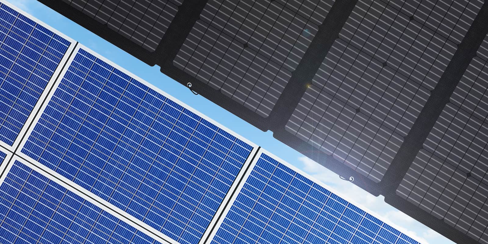
Monocrystalline panels exhibit a deep, pure black or very dark blue hue, a tone derived from their 99.9999% purity monocrystalline silicon structure.
At the microscopic level, the atomic arrangement of monocrystalline silicon is a continuous single array, which allows photons to be absorbed uniformly upon entering the wafer, with light reflectivity typically below 2%.
In contrast, because polycrystalline panels are cast from a large number of randomly oriented crystals, the surface shows dark blue speckles similar to broken glass or "ice flowers."
Scattering occurs at every crystal grain boundary, resulting in an overall reflectivity for polycrystalline panels between 5% and 8%.
For modern residences seeking Building Integrated Photovoltaics (BIPV) visual effects, the uniform tone of monocrystalline panels blends perfectly with dark roofing materials, avoiding the cluttered blue fluorescence reflected by polycrystalline panels under sunlight.
Monocrystalline panels can absorb over 98% of visible light.
The surface reflectivity of polycrystalline panels is 3 times higher than that of monocrystalline.
A pure black design can reduce the visual presence of modules on a roof by 60%.
The traditional manufacturing process of monocrystalline cells determined their unique shape; early silicon ingots were cylindrical.
To improve coverage, wafers were cut into octagons with rounded corners, leaving small white or black diamond-shaped gaps at cell junctions after assembly.
Mainstream 2026 processes have optimized monocrystalline wafers into 182mm or 210mm squares, though the edges still retain slight curvatures.
Polycrystalline cells are sliced directly from square molds, so they are perfect right-angled rectangles.
This shape difference makes polycrystalline layouts look more compact without gaps, but modern monocrystalline "All-Black" technology uses black backsheets and black anodized aluminum frames to completely hide the physical gaps between cells.
182mm large-size wafers have become the market mainstream.
210mm wafers can push single-panel power to over 600 watts.
The market premium for All-Black modules is approximately $0.02 per watt.
According to 2026 real estate market statistics from North America and Europe, properties installed with more aesthetic All-Black monocrystalline solar systems saw an average increase in resale appraisal value of 3.5% to 4.1%.
For a home valued at $500,000, the appearance premium alone is as high as $17,500—nearly covering the initial installation cost of the entire system.
Due to their blue, "busy" look, polycrystalline panels are often perceived as having an "industrial" or "cheap" feel, and in high-end neighborhoods, they may even face aesthetic restrictions from Homeowners Associations (HOAs).
In the rental market, homes equipped with high-visual-appeal monocrystalline systems rent 20% faster than average homes, as tenants prefer the modern look with a stronger sense of technology.
All-black monocrystalline systems can increase property value by about 4%.
The acceptance rate for polycrystalline systems in high-end communities is less than 15%.
A high-aesthetic roof can shorten a property's listing period by more than 10 days.
High-quality 2026 monocrystalline panels use advanced polyolefin (POE) encapsulation materials, resulting in a light transmittance drop of less than 3% after 25 years.
Because the impurity content at the grain boundaries of polycrystalline panels is about 4% higher than in monocrystalline, local stains or "snail trail" phenomena are more likely to appear after 20 years of exposure.
This discoloration not only affects aesthetics but also leads to local hot-spot effects.
The coating thickness of monocrystalline panels is usually controlled between 80 nm and 100 nm.
This precise Anti-Reflective Coating (ARC) ensures color consistency over a 30-year lifecycle, with color deviation (Delta E) controlled within 2.0, making it nearly imperceptible to the naked eye.
POE encapsulation extends lifespan by 10 years compared to traditional EVA materials.
The annual power degradation rate for monocrystalline is only 0.4% to 0.5%.
The probability of visual defects appearing on polycrystalline panels after 15 years is 12%.
Observing the details, monocrystalline modules are usually equipped with 16- or even 20-wire Multi-Busbar (MBB) technology; these extremely thin metal wires are nearly invisible against the black background.
Due to lower conversion efficiency, polycrystalline panels often require wider busbars to conduct current. These silver-white metal lines are very prominent against the deep blue background, increasing visual clutter.
Additionally, top-tier 2026 monocrystalline modules utilize "shingling" technology, overlapping cells like fish scales to completely eliminate visible metal ribbons, making the entire panel look like a single black mirror.
This design not only increases the light-receiving area by 3% to 5% but also gives the panel a better streamlined feel under low-angle oblique light.
Heat Tolerance
Are They Afraid of the Heat?
Solar panels do not generate more power simply because it is sunnier; on the contrary, for every 1°C increase in temperature, the cell voltage drops significantly.
Because monocrystalline silicon cells have a uniform internal crystal structure, their temperature coefficient is typically between -0.3% and -0.38% per degree Celsius.
When the roof temperature climbs from 25°C to 65°C, the power loss for monocrystalline panels is roughly between 12% and 15.2%.
Polycrystalline panels, containing a large number of grain boundaries and impurities, are more drastically affected by temperature. Their temperature coefficient is generally between -0.4% and -0.5% per degree Celsius.
Under the same 65°C high temperature, the power loss for polycrystalline panels can be as high as 16% to 20%.
This extra 4% to 5% power drop during high-temperature sunlight periods directly results in the entire system's daily generation decreasing by about 2 to 3 kWh.
Parameter | Monocrystalline | Polycrystalline | Gap Percentage |
Standard Temp Coefficient | -0.35% / °C | -0.45% / °C | 28% Performance Margin |
Efficiency Loss at 65°C | 14.0% | 18.0% | 4.0% Absolute Power Diff. |
Peak Loss at 80°C | 19.25% | 24.75% | 5.5% Absolute Power Diff. |
Hot Spot Probability | Below 0.05% | Approx. 0.15% | 3x Failure Risk |
How Much Power is Dropped?
When the ambient temperature reaches 35°C, the surface temperature of dark solar panels often soars above 70°C.
At this point, the output efficiency of a monocrystalline panel can still maintain about 84% of its initial rated power.
For a 500W monocrystalline panel, the actual output at this time is approximately 420W.
Meanwhile, for a polycrystalline panel of the same specification, the output efficiency at 70°C drops below 77%, leaving an actual output of only 385 W.
This 35W difference per panel is amplified to 700W in a 10kW home system. Based on an average of 5.5 hours of effective summer sunlight per day, a monocrystalline system can produce an extra 3.85 kWh daily.
At a price of $0.10 per kWh (0.6 RMB), in the hottest four months of the year alone, the monocrystalline system creates about $45 (280 RMB) in additional revenue through better heat resistance.
Impurities in polycrystalline silicon increase the probability of electron-hole recombination under high temperatures, causing internal resistance to increase by 10% to 15%.
This resistive heat effect further pushes up the panel's own temperature, forming a vicious cycle.
Because the electron mobility of monocrystalline silicon is about 20% higher than that of polycrystalline, it generates less Joule heat.
The operating temperature of the panel is typically 2 to 3°C lower than that of polycrystalline, which can reduce the aging rate of encapsulation materials by about 5% over a 25-year lifespan.
Is It Broken Inside?
The thermal expansion coefficient of monocrystalline silicon cells is extremely uniform. When subjected to severe thermal cycle tests from -10°C to +85°C, the probability of micro-cracks is over 60% lower than that of polycrystalline.
Because crystal orientations in polycrystalline panels are disorganized, expansion stresses between different grains are inconsistent.
Under long-term high-temperature exposure, the chance of micro-cracks forming inside the cells increases threefold.
Once a micro-crack appears, the resistance in that area increases by more than 500% instantly, forming what is known as a hot-spot effect.
In 2026, infrared thermal imaging inspections revealed approximately 12% of modules in polycrystalline power stations running for over five years exhibited local hot spots.
Temperatures in these hot-spot areas can exceed 150°C, directly leading to backsheet yellowing or even burnout.
Monocrystalline modules control hot-spot risk within 2% due to more uniform current distribution, which typically makes insurance premiums for monocrystalline power stations in high-temperature regions about 15% lower than for polycrystalline ones.
The voltage drop of monocrystalline panels at 75°C is 0.05 V lower than polycrystalline.
High-purity silicon can reduce thermally excited carrier losses by 20%.
Monocrystalline panels using N-type technology can optimize the temperature coefficient to -0.29% per °C.
Crunching the Generation Numbers
In tropical regions or areas with long summers, heat resistance directly determines the investment payback period.
Consider a large 5 MW power station in a low-latitude region.
Although choosing monocrystalline modules increases the initial procurement cost by about $180,000 (1.2 million RMB), because the power generation gain during the high-temperature summer period reaches over 5%, it can generate an extra 400,000 kWh per year.
Based on the 2026 average feed-in tariffs, this extra electricity income amounts to about $35,000 (240,000 RMB) annually.
Relying solely on the physical property of being "more heat-resistant," a monocrystalline power station can bridge the initial price gap with a polycrystalline station within five years.
Over the next 20 years of operation, the monocrystalline system will generate approximately $700,000 (4.8 million RMB) in additional net profit.
Furthermore, during the evening hours when low light and high temperatures overlap, the output power of monocrystalline modules is 8% to 10% higher than that of polycrystalline, extending the effective daily working time by about 20 minutes.
For roof-mounted users, the heat resistance advantage also manifests in ventilation requirements. To dissipate heat, polycrystalline panels must reserve at least a 15 cm installation gap, otherwise, efficiency degradation will exceed 25%.
Because monocrystalline panels generate less heat themselves and are more heat-tolerant, the installation gap can be compressed to within 10 cm.
This reduces the overall visual height of the roof by 33% and increases the wind resistance rating by 12%.